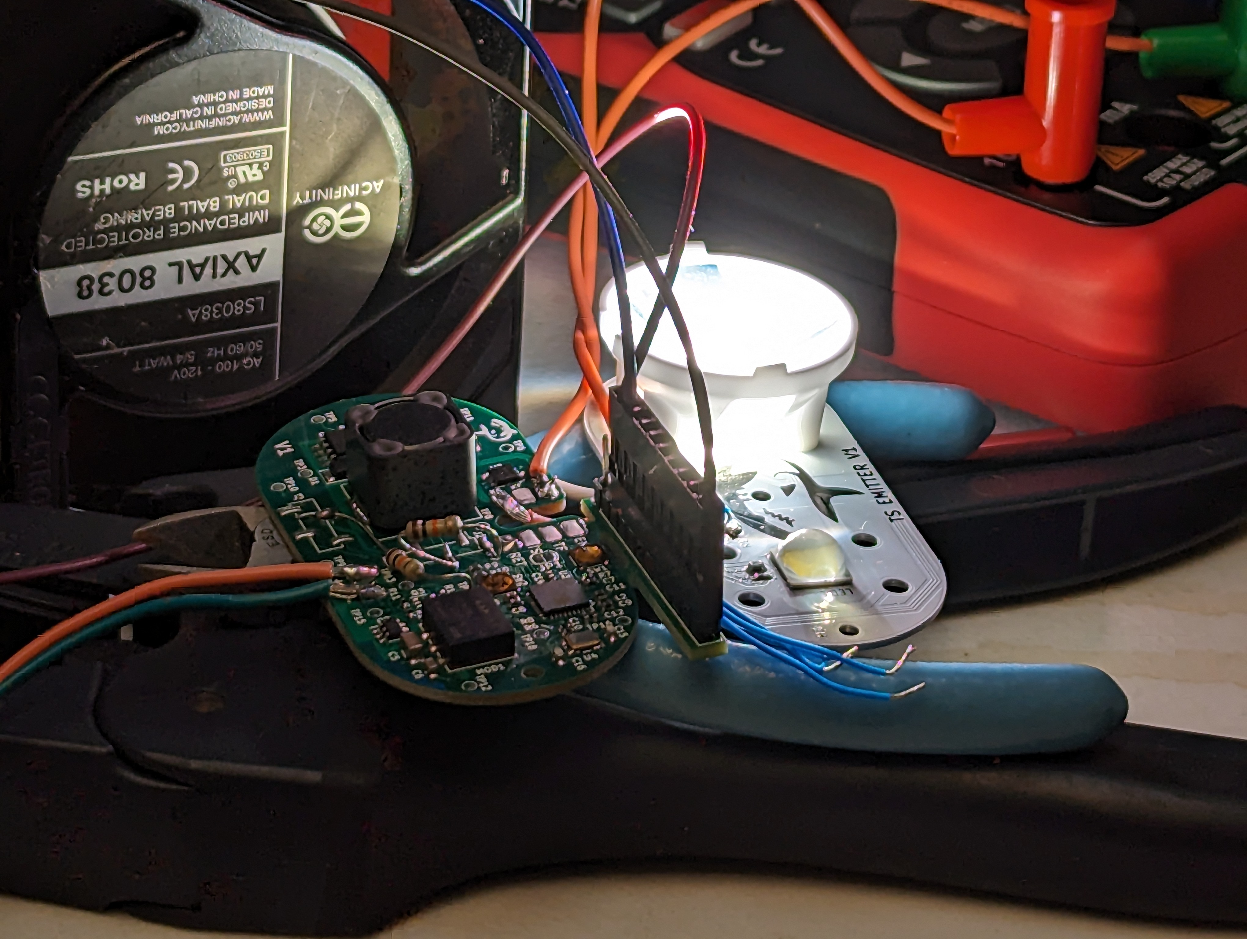
With the dive light parts in hand and assembled, it was time to test it out and fix all the inevitable mistakes. I expected this to go pretty well, and bringup for most low power functions was a breeze- however, at higher currents, this thing is a pretty good heater. This led to buying a fun tool – a thermal camera!
ESP32 bringup:
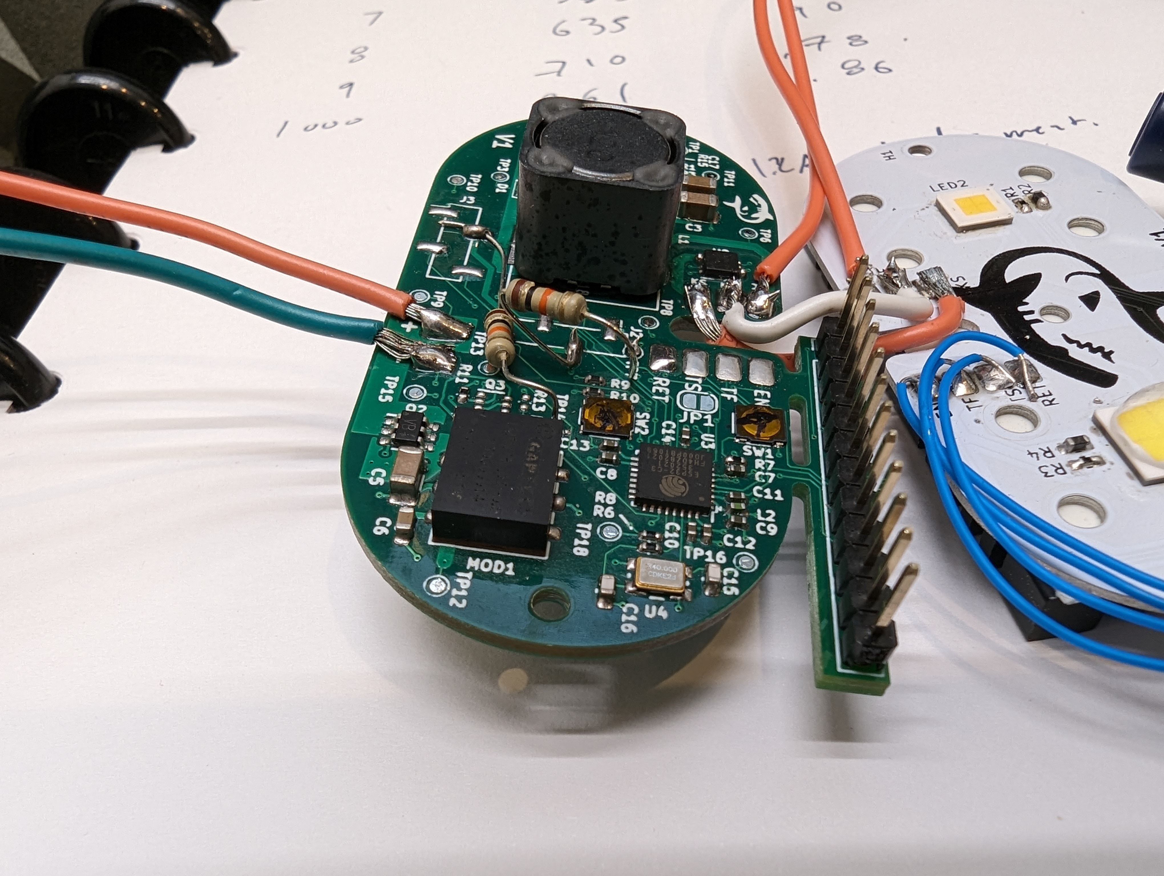
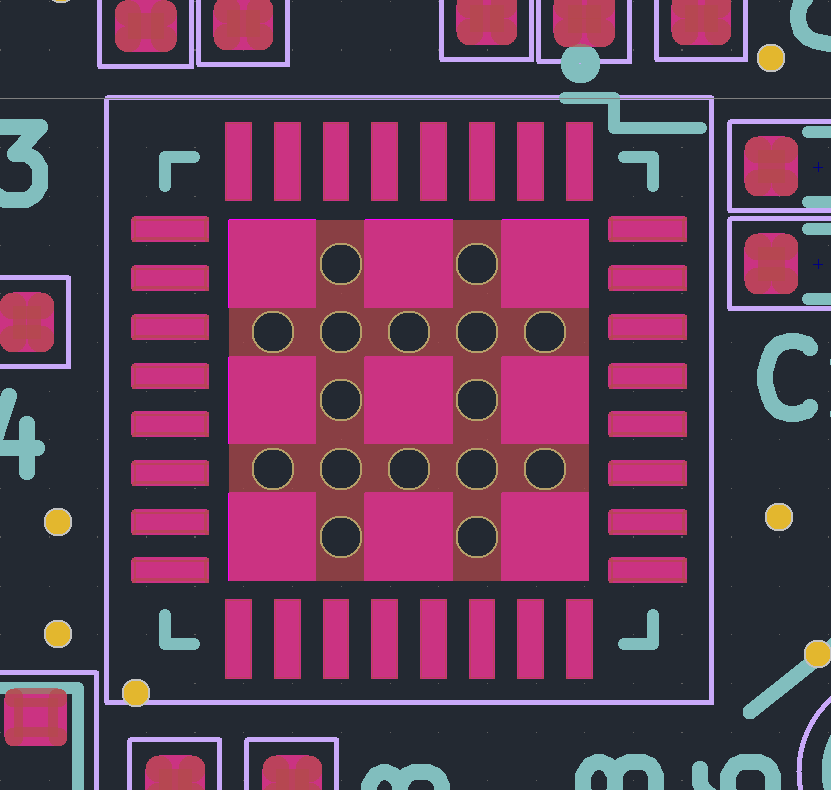
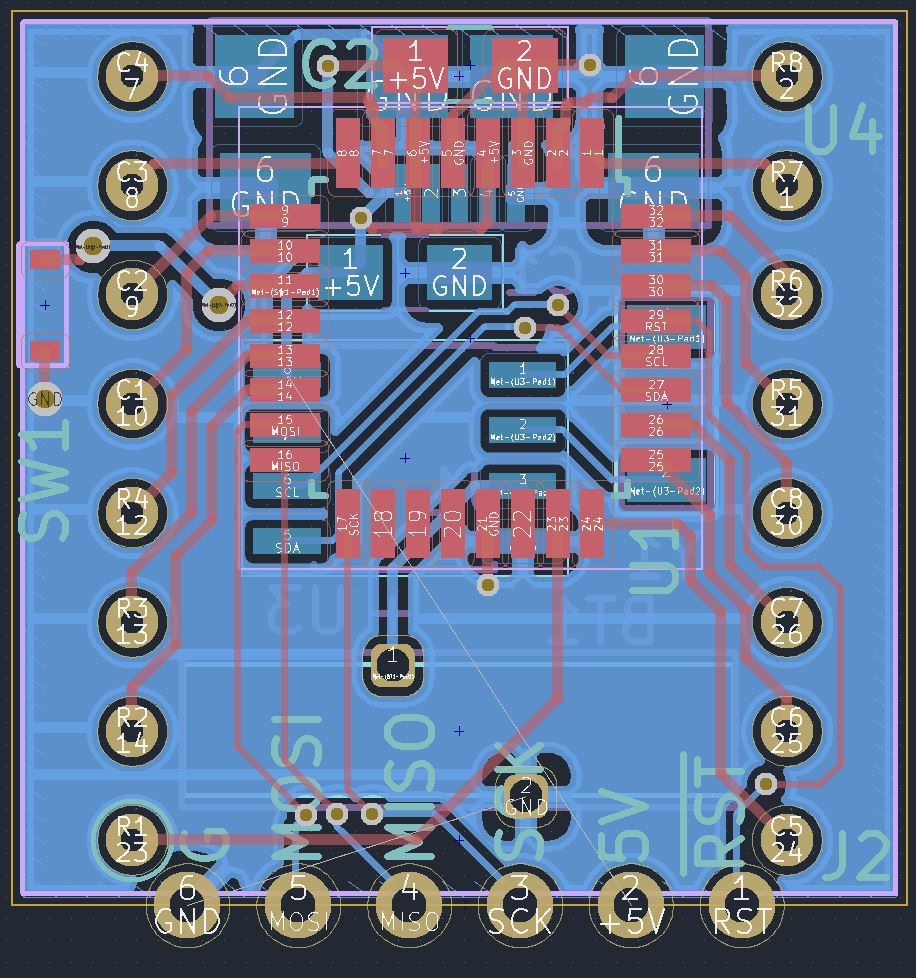
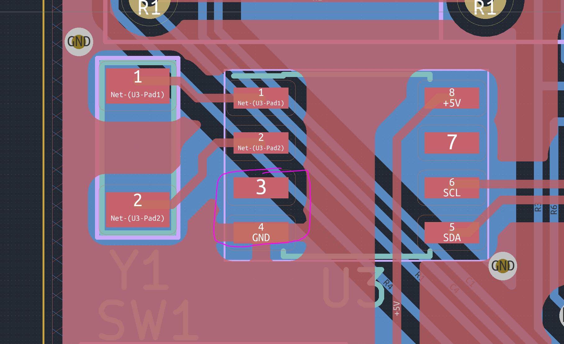
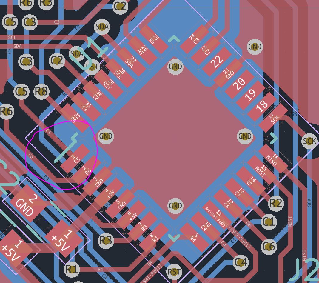
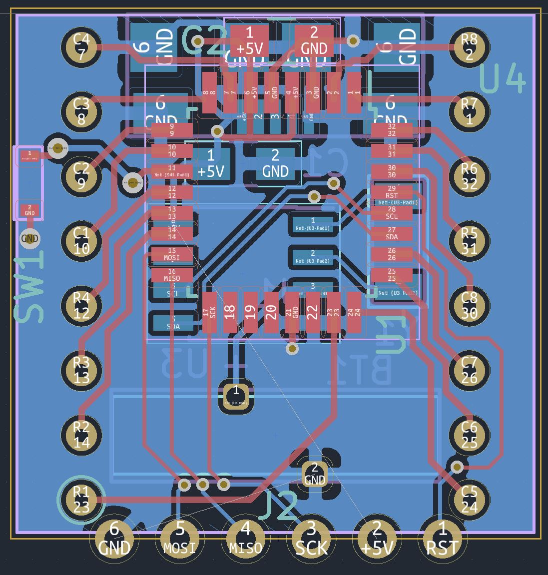
This was my first bare-chip-down ESP32 design, and it was actually pretty easy to do. I used the variant with internal flash to save room, so the only external components were a crystal + caps, some passives (R’s and C’s), and a switch for the RESET line, and a switch on the BOOT (gpio 9). However, there are two additional strapping pins (GPIO 0 and 2) that needed pulldowns. This was annoying since these pins were not pulled down on the pcb – some of them were pulled up, so the parts that did that needed to be removed, and the functionality of those circuits needs to be checked some other way.
I think in the future, it would make sense to avoid using the actual boot and reset buttons and use something like the ESP-PROG to toggle all the lines. Needing to push buttons to upload code is a drag!
pink=paste. This footprint has too much
I also consistently had issues soldering the QFN package the ESP comes in- I think this was due to too much paste on the center thermal pad. This causes the chip to float, and sometimes this causes one side of the chip (or a few pins) to lift. Next time I will reduce the amount of paste on the center pad to fix this, but I resolved it here by removing the chip, solder-wicking the thermal pad, and then re-soldering the part. Using low temp solder paste made this really easy.
LM3409 Driver bringup:
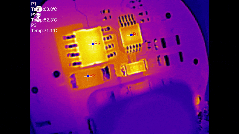
The LM3409 bringup went relatively well, but thermal issues started to crop up pretty much immediately. There are some surprising deficiencies in the layout and parts that I will be modifying for future revisions. The thermal camera really helped to visualize the issues quickly, and given the number of thermal/power projects I have worked on recently I am sure I will get to use it quite a bit.
PFET Gate Charge
One hair raising issue was that during bringup, the board started to smoke. This is almost always a bad sign. In my original estimation, this was caused by the buck PFET getting hot due to having a high gate charge. The odd thing is that the freewheel diode also got really hot, and stayed hot even if the led was very dim.
A very basic thermal investigation with two thermocouples showed that the FET was getting hotter than the diode, at least initially. However, I did smoke several diodes in the process.
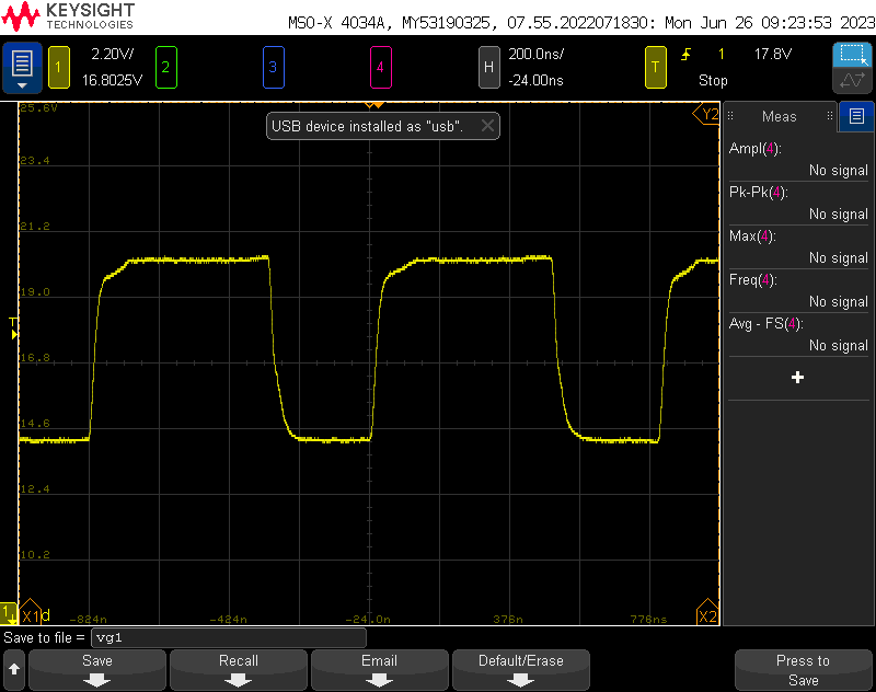
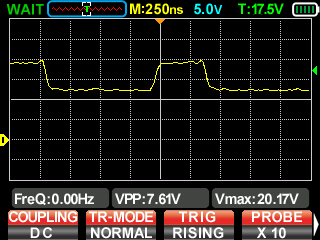
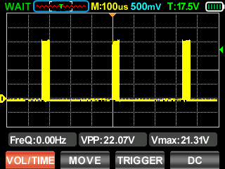
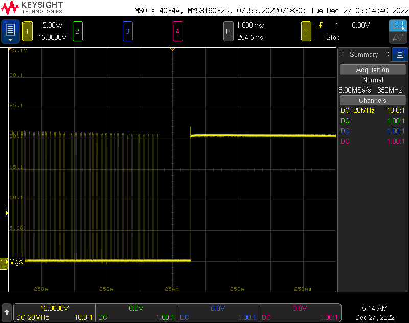
original fet gate voltage. roughly 200 ns of switching time.
Reducing the gate charge did appear to solve the problem, and there was even a note in the datasheet (that I glossed over) about keeping the gate charge below ~30nC. Having a high gate charge is problematic for two reasons- it keeps the FET in a high RDS region for longer during switching, and it requires more power from the gate driver on the LED controller, which also heats up. However, this was not the real problem.
Overheating and Limp Mode:
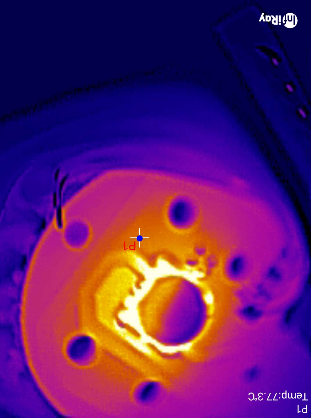
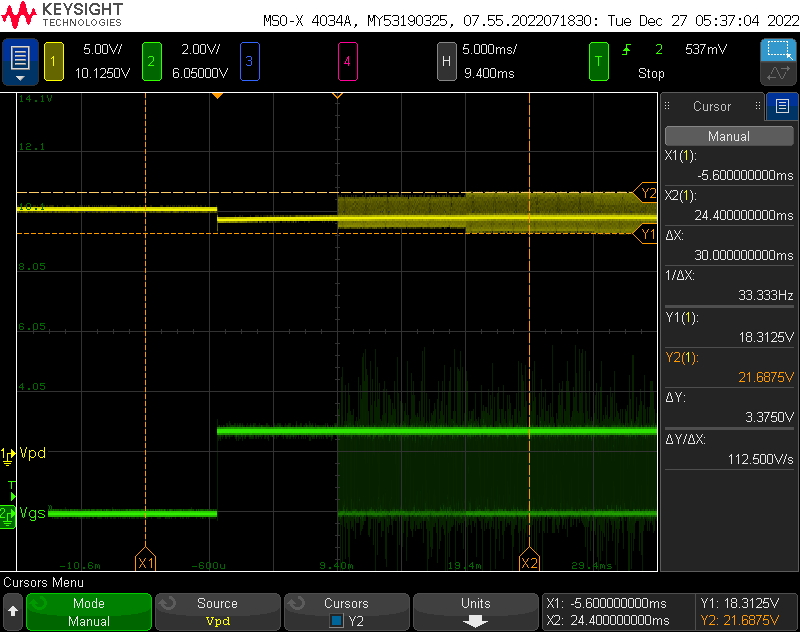
Note that initially P1, the driver heats up to ~70C. Once the driver gets hot, P2, the diode, gets VERY hot (150C!)
Gate charge was not the entire story. With the FET replaced with a lower gate charge/higher RDSon model, there was still an issue! With the LED aggressively cooled (to allow it to live), the device would still go into some kind of limp mode after a few minutes of operation at high currents (3.6A avg, 12V, about 42W).
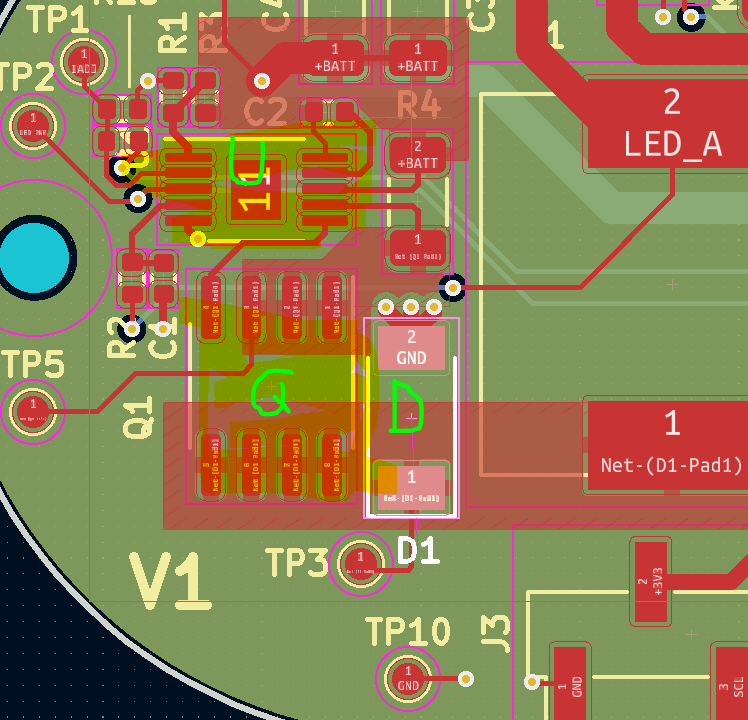
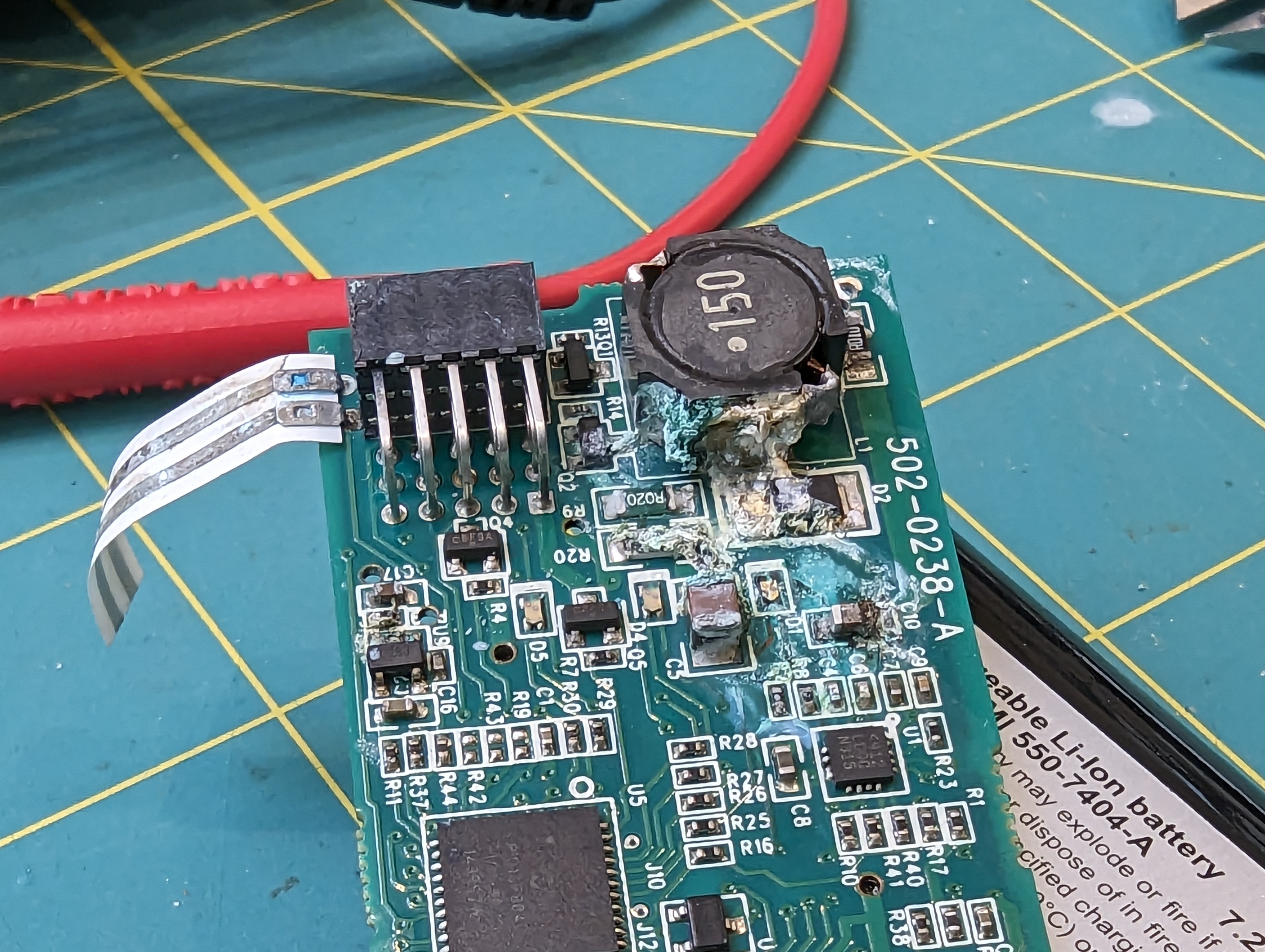
This seems to be due to the driver itself overheating, which is due to my poor thermal design. The driver is marked U in the layout above- this is supposed to have a thermal pad connected with vias to ground. I omitted the vias, essentially insulating the chip- no good.
Gate Voltage
Second, at high currents, the regulator needs to switch frequently to keep in regulation. Estimating from the gate voltage above (in terms of time), and assuming maximum 1A gate drive currents, I estimate that the total switching time is at least 100nS with a period of about 1375nS. The average voltage is about 16.5V, so 16.5V*1A*D = ~1.2W. This would probably be easy do dissipate if I hadn’t insulated the chip. Reducing gate charge helped reduce the power this chip was dissipating, but it was not the root cause.
To make things worse, I didn’t add much copper to dissipate heat on the FET, and at least half the copper is on the side of the driver, which actually makes things worse (its easier to for the FET to heat the driver). Adding some vias to a large plane on the back, and increasing the area on the front will increase the area the heat can easily dissipate from.
The reason the diode gets hot is because usually, the diode only free wheels for a short amount of time- when the FET is off. When the driver goes into limp mode, it has to dissipate all the energy stored in the inductor, many times a second.
So the full story is- this driver will self destruct if the driver overheats and goes into hiccup mode. Better thermal design (and eventually cooling it in the ocean) will probably improve the situation, by preventing driver overheating.
A wiser choice of package for the FET might also help dump heat to the PCB, which will be important when this is running in an enclosure. Convection won’t be an option then, and all the heat will need to go into the case.
Efficiency + Thermals:
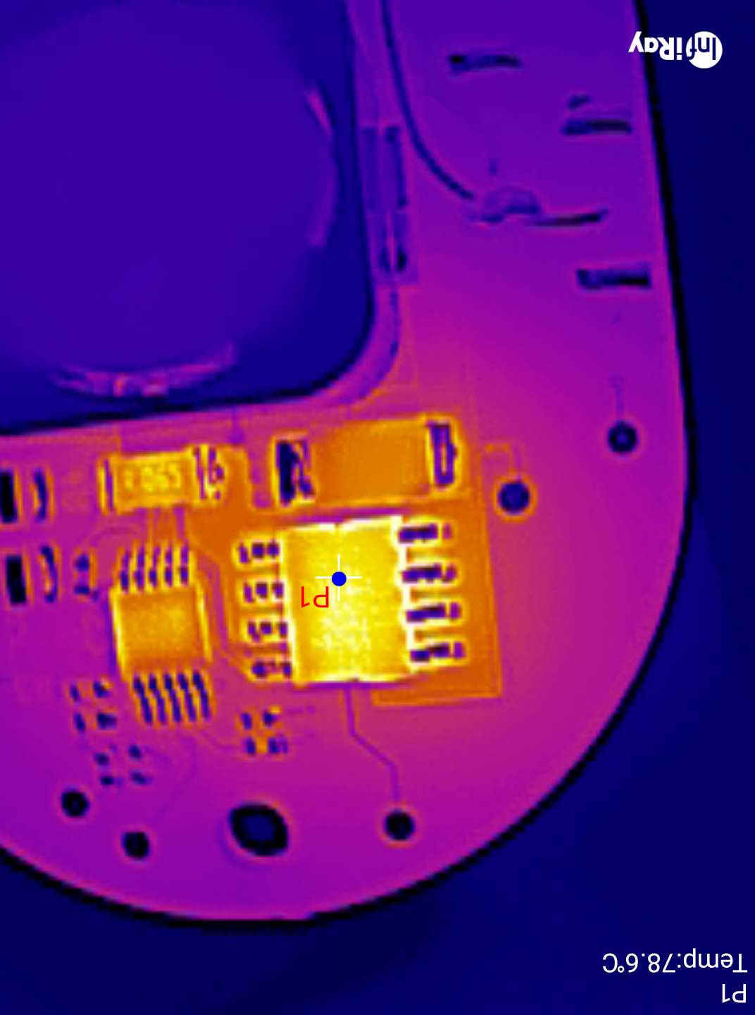
With the driver sorted, the next thing to do was to smoke test the lamps at high currents. This went reasonably well, with only one LED burning out. As you can see above, the XHP70.3 required a heat sink and passive water cooling in order to prevent burnout. Given that its running at about 42W and only ~25% of the energy is turning into light, this is a 32W heater in a 70x70mm footprint.
This is at about 70C
This is going to be very hard to keep cool, even with the die almost being in contact with the seawater. The good news is at lower settings (around 2A) I should still get a very respectable 3000 lm out of the LED- more than the sola light!
Overall efficiency from power supply to LED was acceptable- in the mid 90’s for lower currents up to about 1400mA, and in the high 80’s above that. while that might seem like poor efficiency, this takes into account relatively long lead wires to and from the pcb, the multimeter, etc, so I actually expect it to improve in the final product, especially once the thermal design is improved.
Conclusion:
This PCB needs to be re-routed with thermal concerns and strapping pins in mind, but overall, it works! This iteration has given me a lot of confidence that the final design will do what I want it to do. I’m also really excited to keep playing with the thermal camera. It gives me a lot more information than the sizzling finger test, and it lets me dig into the context and sequence of the heating.
I recently found out my sola 2000 torch is torched- water got in and corroded the connectors. while it might be technically salvageable, I used this as an excuse to start another project- a canister dive light. I love my sola light, but the battery does not quite last two dives, especially at full blast. This means I need to bring two lights, two chargers, and two lights, and that is a little inconvenient. It also means I spend a lot of time futzing around underwater going from low to high power mode. This is surprisingly annoying, especially since I have to use two hands to switch modes.
Armed with google, hubris, and kicad I set out to design my own dive light.
Design Goals:
The goal is to build a dive light, with spot and flood modes, just like the sola lights. I want a burn time of at least 3 hours at a reasonable brightness- this is well over two recreational dives. I want it to be a canister light so I can run it full blast for the whole dive, temperature permitting. And I want it to be about as bright as the sola lights. And small. And I want a pony to go with it (kidding).
Optics and LED choices
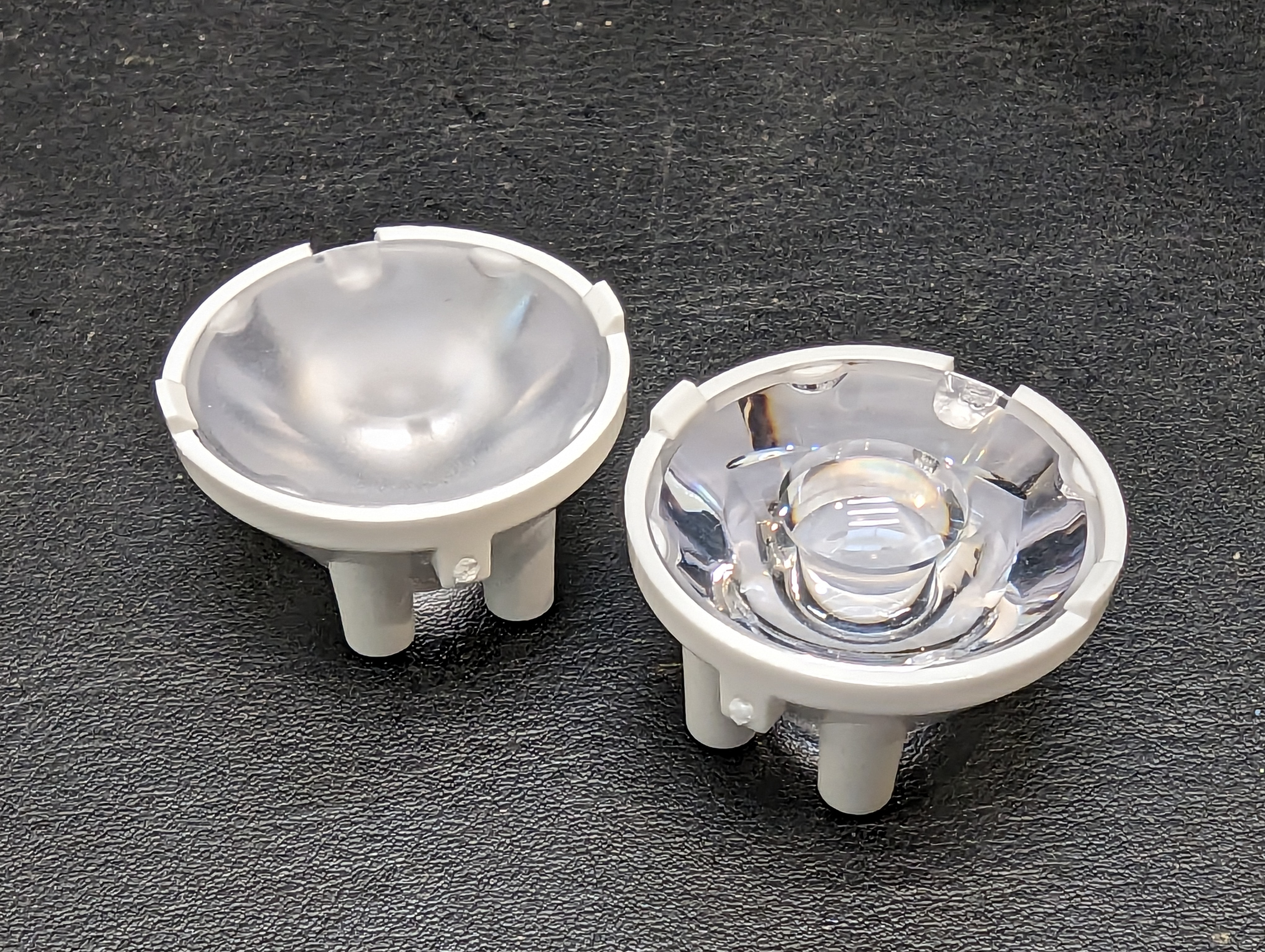
There are a lot of constraints on this project, starting with thermal and optical considerations. There are only so many off the shelf optics, and without much in the way of a mechanical prototyping department, I want to minimize iterations. The simplest way to do this was with single LEDs and off the shelf optics. Carclo has not only an impressive array of parts to buy, but they also have charts/images to go with the optics with different base LEDs.
The problem with single LEDS is that the efficiency of the LED suffers at high outputs. This creates a lot of heat. Hopefully I can use the ocean as a heatsink. CREE seems to make hands-down the best high output LEDS, and after some careful considerations of what is available in low quantities, I decided on one XP50.3 and one XP70.3 LED. Two XP70.3’s would be better, but the beam pattern on the spot light would be too wide, since I can only get the XP70.3 with a dome lens.
Driver
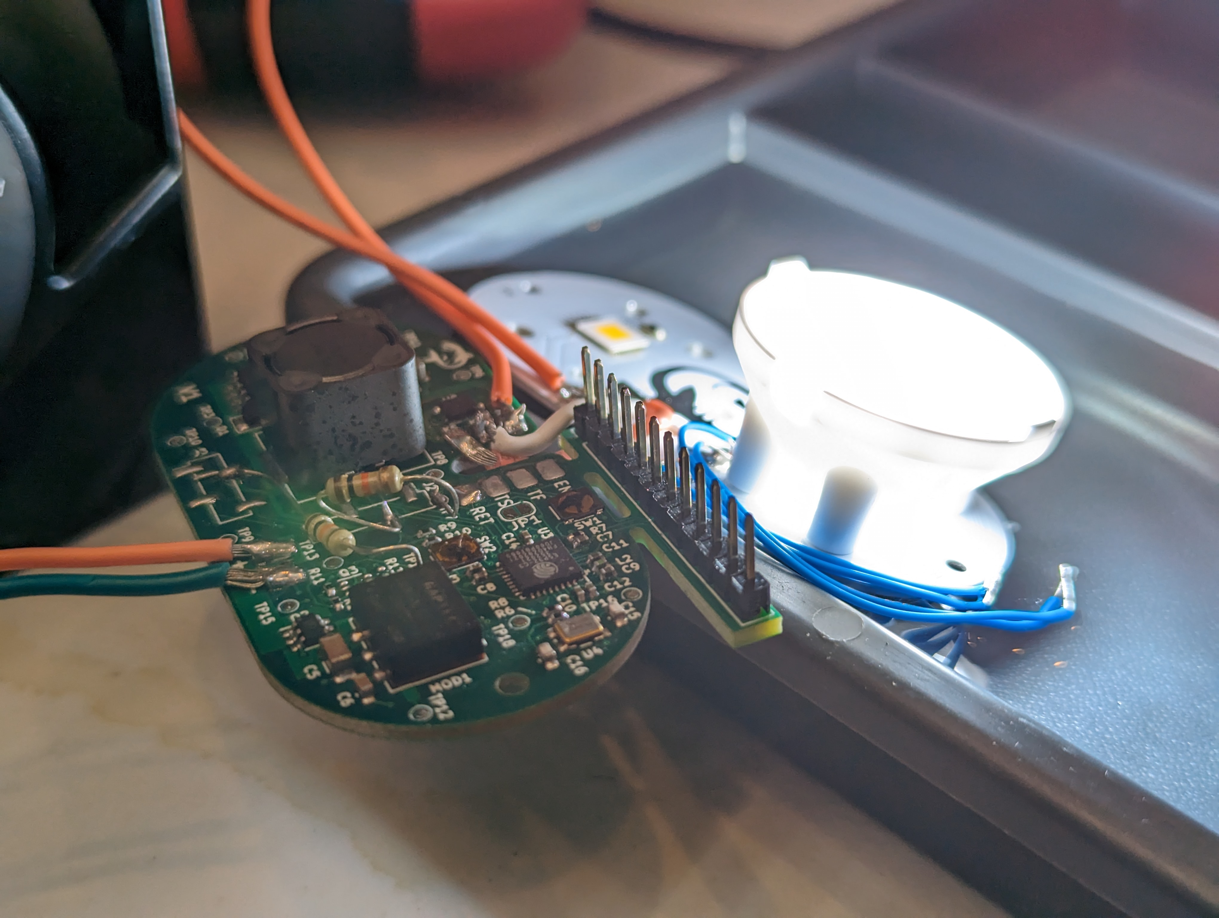
Next up was the driver. It seems pretty useless to have spot and flood lighting on at the same time, and as you can see, the PCB does not have a lot of room on it for another big driver and inductor. Instead, I intend to share the high-side LED driver across both LEDs by low-side switching them. The header on top is for programming, and as a breakout for interesting pins.
Microcontroller Selection
I begrudgingly picked the ESP32 as my microcontroller. It seems like a shame to have and not use a ton of the peripherals on there, but its cheap (compared to an attiny), small (but still has a lot of pins), and in stock (unlike the atsamd series). This requires a 3v3 regulator, and due to size and laziness constraints I opted for an integrated DC-DC module. These are awesome, cheap, and easy to assemble, which is nice because I already had a lot of 0402 parts.
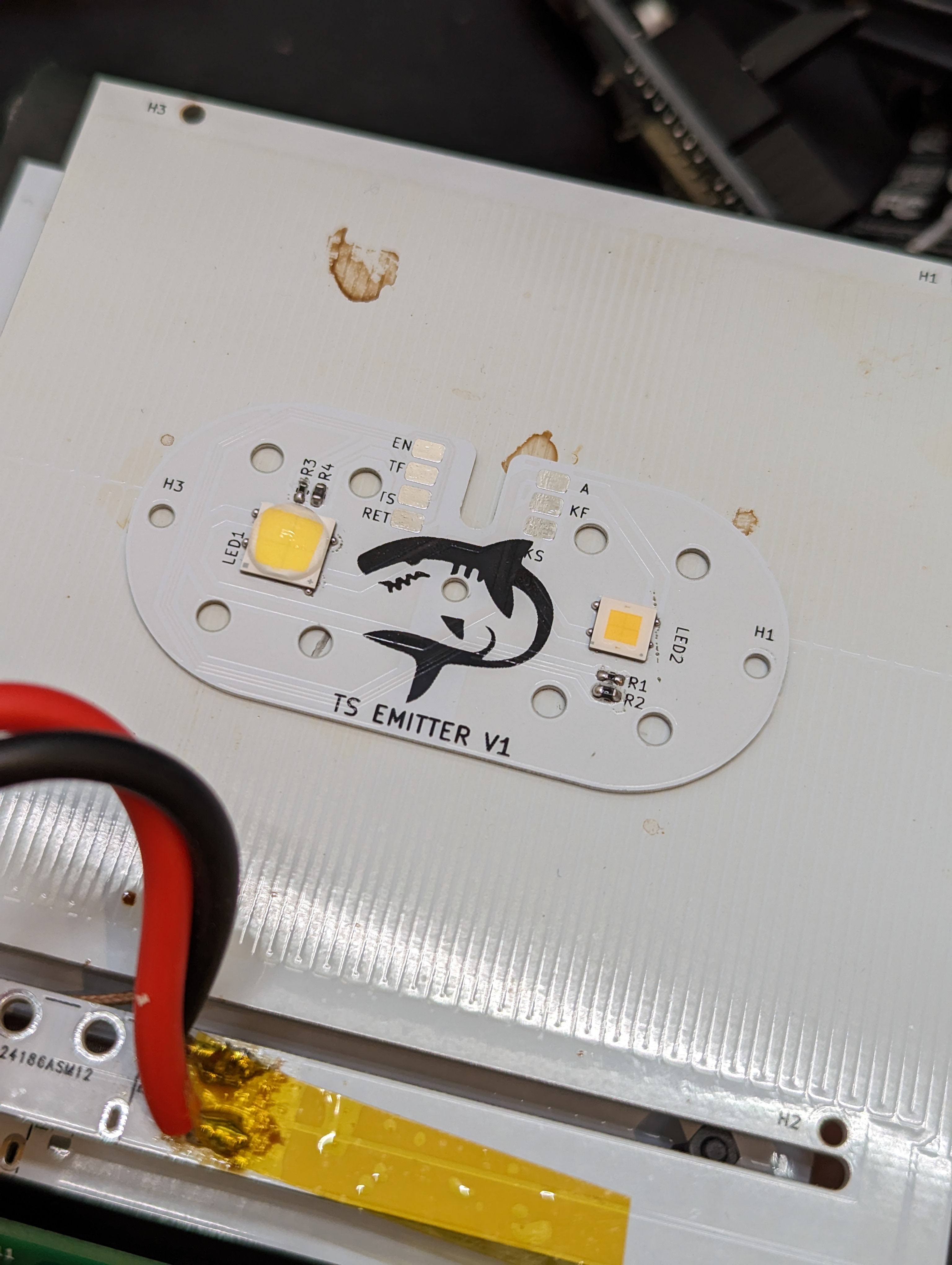
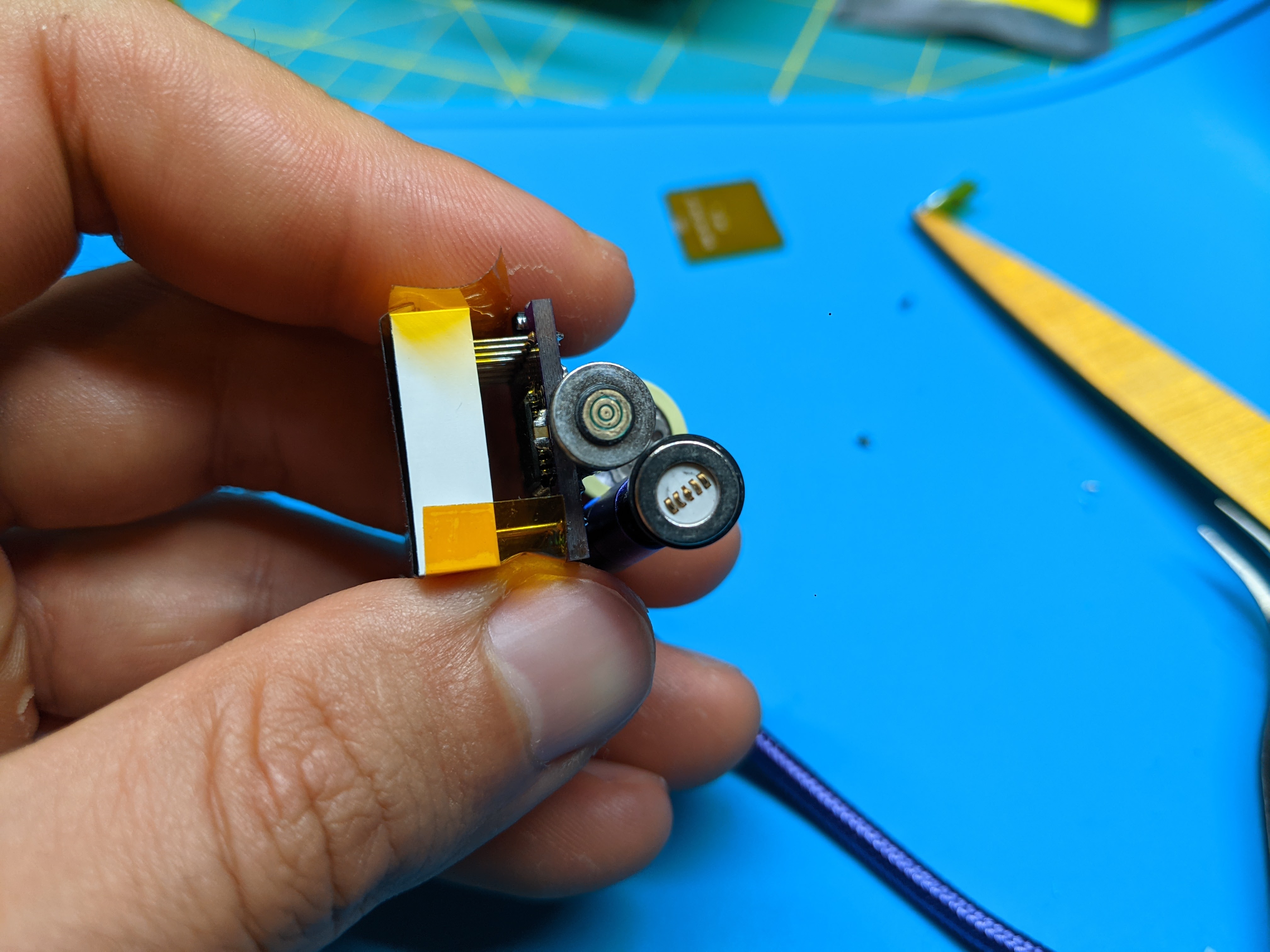
Emitter (LED) Board
The emitter board is aluminum, for better heat conductivity. At full blast, this will need to dissipate ~30W! In addition to LEDS, there are a couple thermistors for temperature measurements, placed near the LEDs. Given that each LED is a multi-watt heater that could probably melt itself off the board (with low temp solder), it seems prudent to monitor temperatures.
The hot plating continues! And with the boards actually in hand, I can compare my estimates to some real world measurements.
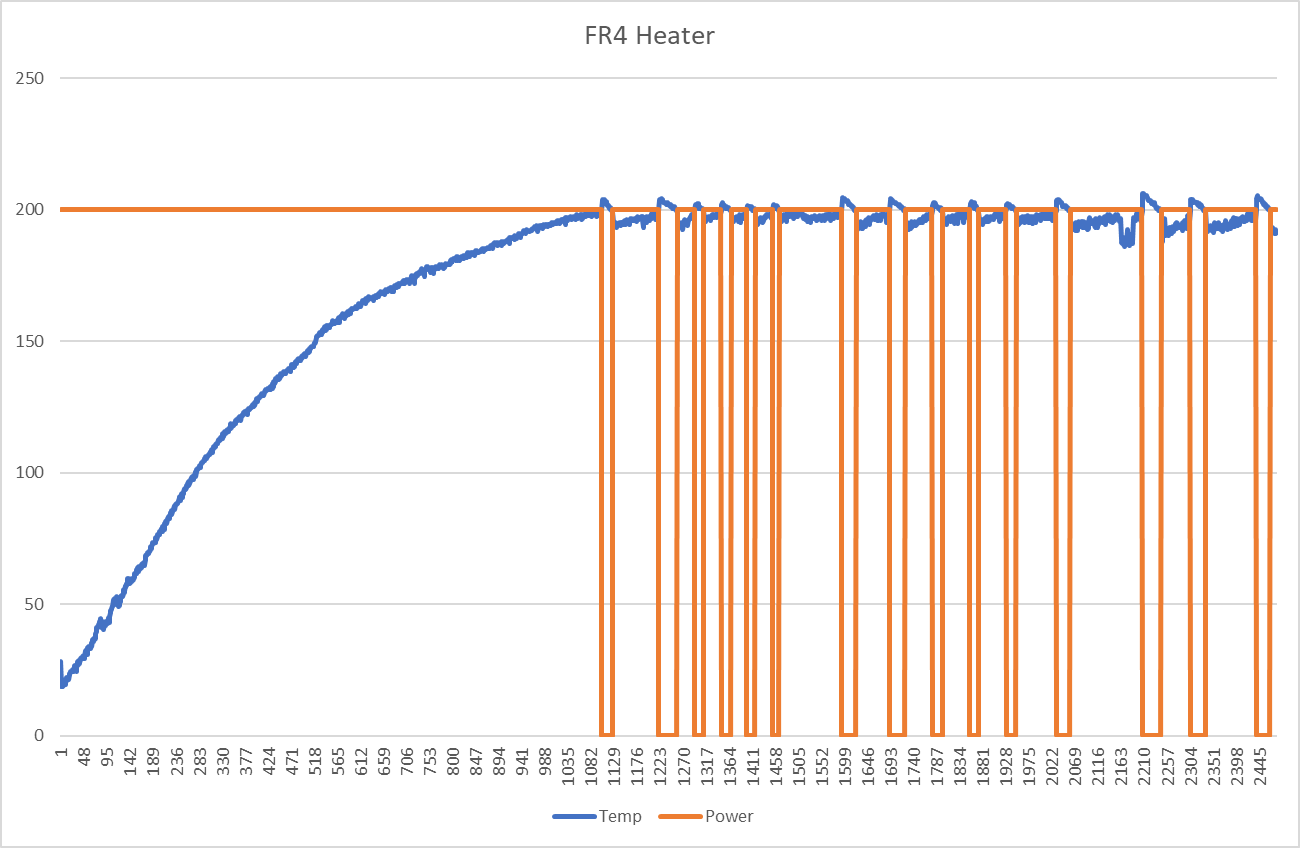
In the end, I made both FR4 and aluminum heaters. These heaters ended up having slightly different properties. Oddly, the aluminum PCB has a higher resistance (4 ohms) than the copper pcb, 2.9 ohms). Read on to figure out what this did to the design.
Designed Vs Measured Resistance:
The design resistance of the heater track was 3.3 ohms. Clearly, this was not “nailed” for either of the boards, but it was close. I was surprised that both boards didn’t overshoot the resistance, due to the addition of a few extra squares of conductor on the connector island- however the FR4 heater seems to have a more generous allotment of copper, and the aluminum PCB may have slightly less copper.
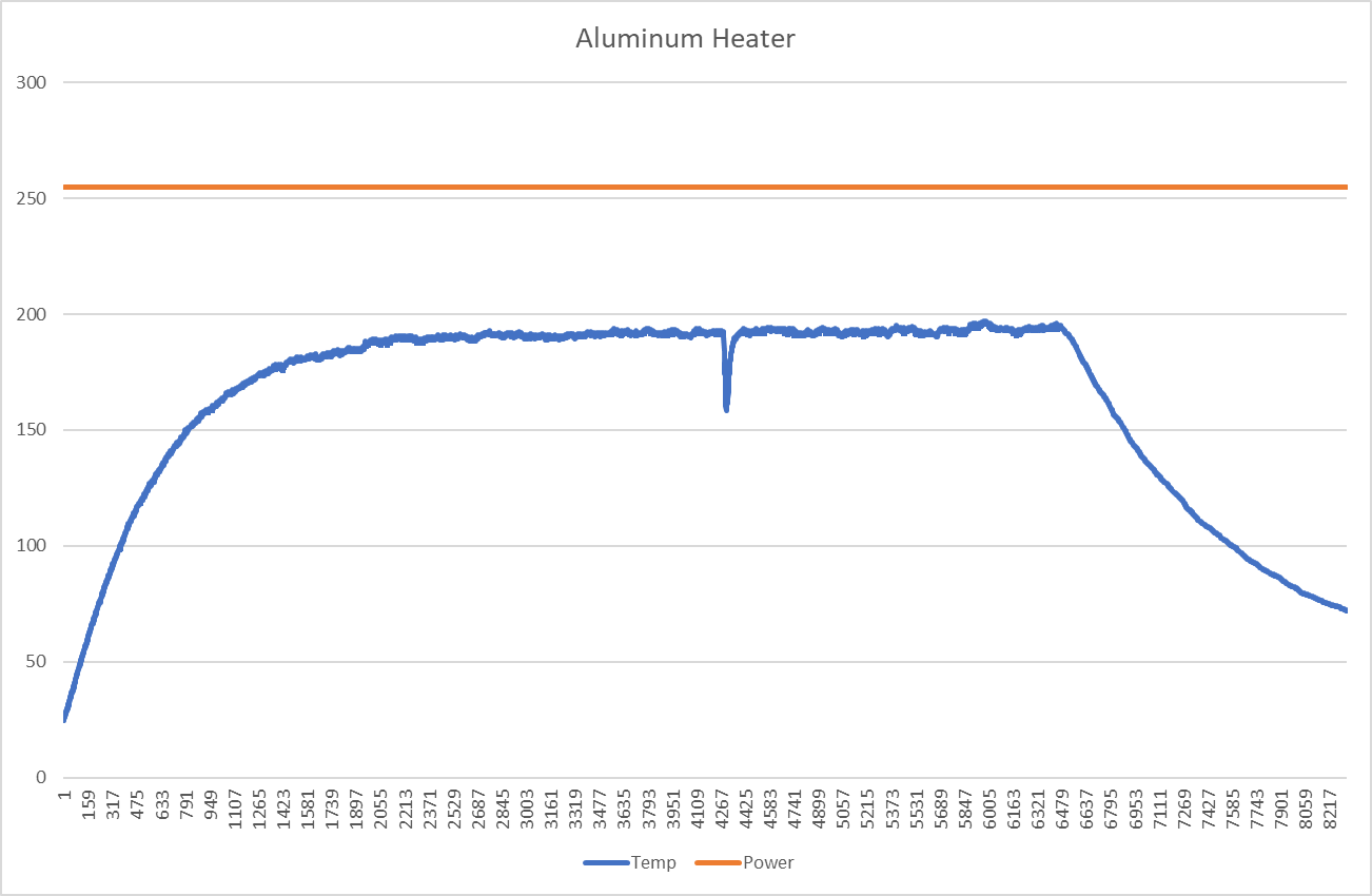
Unfortunately, this means that at higher temperatures, the power delivered to the aluminum board is much lower than desired. The calculated value for the resistance at 200C is about 6.7 ohms, and the measured value is 7-8 ohms. This means that the maximum power available at 20V is 50-60W, or less. This is pretty close to the theoretical minimum power needed to reach 200C, which is why this plate struggles to achieve 200C. As you can see, the heater is on for the entire time (until I pulled the plug). Time units are in 10ms intervals. Fortunately, this validates the power delivery assumptions I made in the past post.
To recap, Qdot is the amount of heating power needed to sustain a particular delta T, given some convection parameters. I assumed a delta T of 175k, with an area of about .01m2, and h being 25 W/m2k, resulting in a power delivery at the heater of 43W. while this is not totally spot on, its in the right ballpark. It suggests that lowering the resistance and actually delivering 100w would be very helpful to removing this 200c limit. I think 10-20 is a reasonable conservative estimate of convective cooling, but its conservative in the wrong direction if you are designing a heater.
On the other hand, the resistance of the FR4 heater is low. At low temperatures, running at 100% PWM (all on), will cause the power supply to brown out. This means that the power delivery actually needs to be cut back (PWM’ed) when the heater is cooler, so that the overall current draw is lower. Once the heater is in the vicinity of 100C, it can be run “full blast”, aka more or less shorted across the power supply.
Does It Blend?
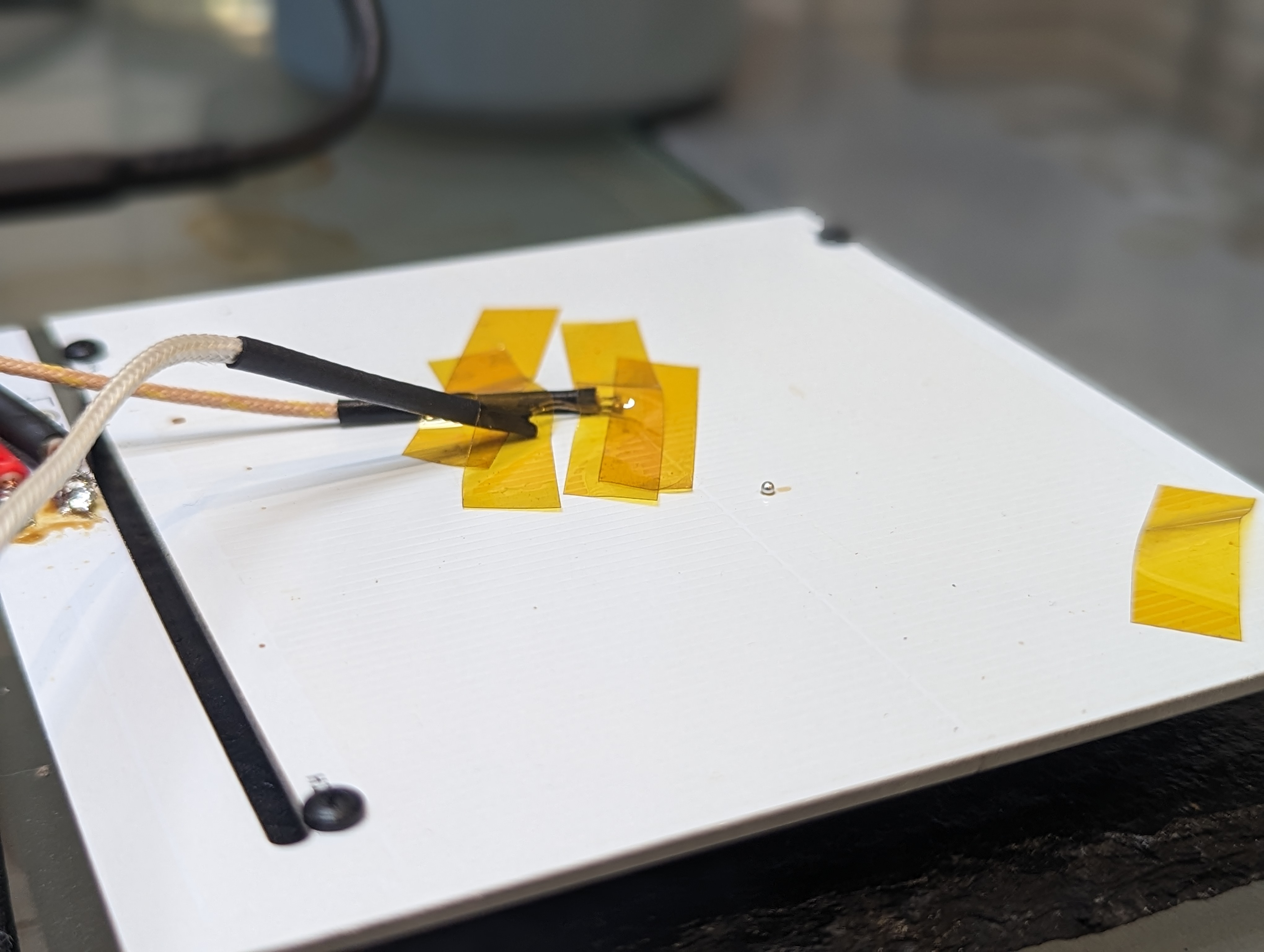
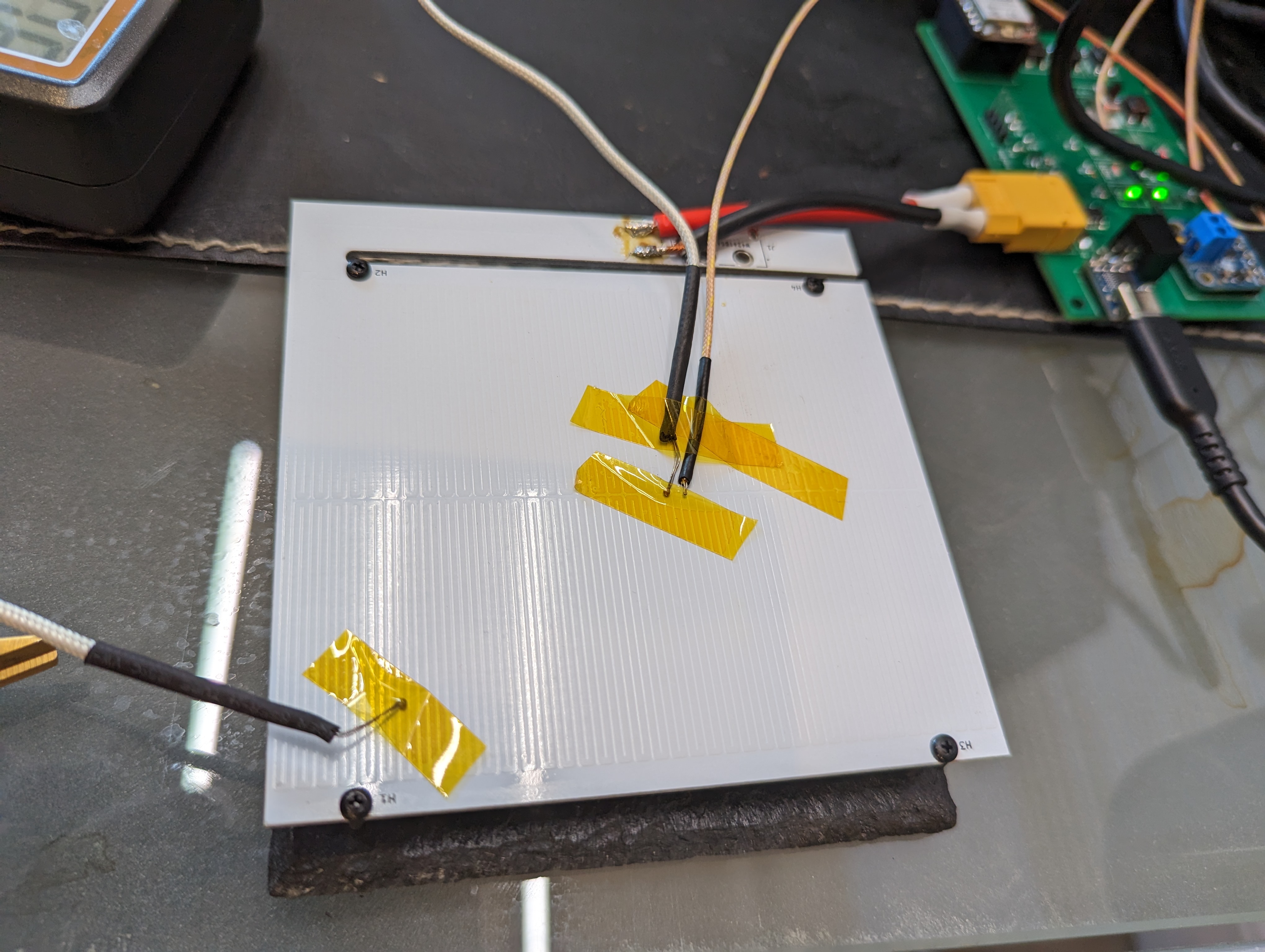
Both the aluminum and FR4 heaters were able to reach 200c depending on the conditions. Both were capable of melting solder directly on the plate, as you can see. The aluminum heater would benefit from an improved (lower resistance) heater trace.
The remote probe feature allows for the sensing of the temperature of the PCB being soldered. This is good, since that is where the temperature actually matters. This can cause the heater to get much hotter (20c or so) than the top of the target board, which in this photo, resulted in some discoloration of the solder mask of the heater.
Temperature Gradients and Overheating:
The hot plate design needs to achieve two tasks: be cold at the connector (so as not to de-solder it), and it needs to be hot (and ideally, evenly hot) across the surface.
The worst case for de-soldering the connector is with the aluminum heater, since the aluminum substrate should conduct heat pretty well. Up at peak temperatures, the connector area only got to about 85C. Certainly warm, but not nearly hot enough to damage the connector.
In terms of heater gradients, the aluminum PCB had about a 10C difference from the center to the corner at 200c. The gradient to the “neck” of the connector island was much worse (13+ C), since the thick traces there (and the substrate) act like a heat sink. The corners are cooler since there is some radiation and extra convection out of the sides of the heater.
The FR4 board has a even higher gradient, in excess of 50C during heat up, and staying steady at about 50C after several minutes. This is annoying, since it makes the outer areas of the PCB too cold to solder on. The center can be overdriven to compensate, but that leads to overheating and discoloring the solder mask.
New Design Goals + Limitations:
Its clear that hot plate soldering is not the ideal way to solder- something like a toaster seems a lot better and faster, since it can more evenly heat the target PCB. The main issue is that in order to get the top of the PCB hot enough to reflow, the bottom has to be quite a bit hotter. This is worse with traditional lead-free solders, since they need to hit about 220C. Lead-Tin eutectic solders need to hit 185 or so, and bismuth lead-free solders only need to reach 140 C (there is a medium caveat here).
You can see the results of this heating on an adafruit board (above), that I gently reflowed. The left board is new from adafruit, and the right one is reflowed. It didn’t really damage the board, but it certainly would be an unacceptable outcome if a manufacturer overheated a board like this, and the lead free solder (I assume) on top barely reached the liquidus point, and would re-solidify as soon as I moved a component.
The medium sized caveat is that any lead in the process can poison your bismuth solders forming a bismuth-lead crystal that has a very low melting point (95C!). I think the jury is still out on using bismuth solder for stuff that gets hot, but for most prototyping it seems fine. For low temperature solders, the hotplate is fine because your whole board stays under typical soldering temperatures.
For leaded solders the hot plate will likely also work ok, since the heater can be at about 200c and the surface of the target PCB can be at 180. However, for lead-free SAC (Sn Ag Cu) alloys, I think the hot plate will likely damage the solder mask of the target PCB. However, using the PCB hotplate as a preheater could work fine, with the addition of a hot air gun assist.
I would like to use this hot plate to solder and test complete prototype designs, with packages that are hard to hand solder, particularly leadless stuff like QFNs. I find solder fumes to be irritating (and there are more at higher temperatures), and so I am going to try using the bismuth solder, at least for prototyping. For leaded work, I’m pretty sure the hot plate would work fine, and it will be a good tool (combined with hot air) for reworking SAC alloy lead-free boards. I’d also like to take up less closet space than a toaster oven, so I think the project does have some value. It also fits in nicely with the USB-C powered soldering iron ecosystem.
Electrical Stuff:
In the previous posts I shared some choices around the electrical system. The two concerns I had were not shorting out the power supply, and preventing inductive spikes from exceeding Vdsmax.
The Vgs, shown above, was totally fine since it was limited by the free-wheeling diode. Even with a 1ms charge time, the inductor failed to exceed 25V and there was very little ringing. The Vdsmax is about 30V, so there is plenty of margin.
To test power integrity, I wrote some code to turn the heater on different power levels for 10ms, starting at 100% power. As you can see, 100% power reduces the output voltage just a bit, to 19.5V. This is well within the PD specification. When the PWM begins, the power supply seems to tolerate some relatively large spikes/dips as the heater (inductive load) is switched at 25kHz.
Electrical + Control Improvements:
To get a truly performant hotplate, the resistance at 200C needs to be less than 4 ohms, so the full 100W (or close to it) can be used to maintain the target operating temperature. Doing this is tricky, because it means that at 25C the heater can’t be operated at 100% duty cycle. Basically, power is not a function of duty cycle, but of duty cycle, temperature, and board characteristics.
There are two approaches to solving this problem. One is a per-heater lookup table, that lists a reasonable safe duty cycle per temperature. This is limiting since it would need to be generated per-heater, but its not unreasonable to do that given that I will likely stick with a single heater, and most heaters should be pretty similar.
Another approach would be to add a current monitoring to the USB PD supply, and cut the heater power off once you get close to the limit. This requires a relatively high bulk capacitance to provide current, even at 25kHz, but its certainly achievable. Overall power could be modulated by adding a dead time in between heating cycles, in order to follow a temperature profile. Higher frequencies could be considered, taking into account the switching time of the low side FETs. This is basically a current-controlled buck converter.
I’ll likely stick to the first approach for now, since doing current limited control requires more hardware, and it is unlikely to really improve the outcome of my soldering.
Mistakes + Takeaways
There were a few minor circuit goofs, and some things that went surprisingly well. Here is a small list, that might help you or me in the future:
GPIO9 and GPIO8 on the ESP32 C3 are bootstrapping pins– they control what the ESP does when it boots. I connected one of them to a switch, as an input for the program. This meant that the ESP would not boot into my program, but it would boot back into bootloader mode (and accept new programs). Toggling the switch made the ESP behave normally. Note to self: use these pins carefully.
The pinecil is a pretty beefy iron. It had trouble soldering to the aluminum PCB, but with boost mode and patience it had enough power to solder directly to a 3mm wide trace on an aluminum substrate. It had NO trouble soldering XT60 connectors to large pours. Don’t let the small size fool you- it is a real iron.
It is a good idea to put indicator LEDs on things like the actual power rail and the actual HEAT signal. It makes it unambiguous that something is really happening, and that the heater is getting hot.
I added a solder jumper to the overtemperature cutoff circuit. I accidentally swapped the inputs on the monitor chip, so it didn’t work. Cutting the jumper made it really easy to test with this protection turned off.
All my temperature sensors gave wildly different readings, even when co-located. I’m not sure why, but I do trust that the delta temperature measurements were ok since they were from the same instrument with two of the same probes, and they had the same readings when physically connected.
USBC-PD can deliver serious power, and its easily obtained with USB PD trigger boards.
Next Steps:
During testing, I learned what this type of soldering setup is really appropriate for, and what the capabilities of the heater are. I want to try some of this low temp solder, and I want to do some hot plate soldering to figure out how it feels, before going back to take another pass at the heater element. I suspect targeting an even lower heater resistance will allow me to hit 200C easily with the aluminum plate.
I also have some work to do on the UI (there is a screen- I just didn’t plug it in), and on the controls. If I find it useful, I will probably build an enclosure for it to protect the electronics and to make it easier to use.
The PCB heater for the hotplate obviously needs to be driven by something. I could have put more circuits on the heater board itself, but separating them has some advantages:
if the heater element is bad, or needs reconfiguration, it can be replaced
better opportunity for a heat break between the boards
opportunity to try different heater substrates or even different heaters/heater shapes
My goal for the hotplate is to keep it simple. I decided that I really probably need one profile at most, and a manual-temperature mode. I’d rather make that profile on the computer, instead of on the device, and be able to play it back from the device. I’d also rather get information back from the plate on the computer instead of a tiny display. Hopefully these simplifications will allow a hotplate to be up and running sooner rather than later.
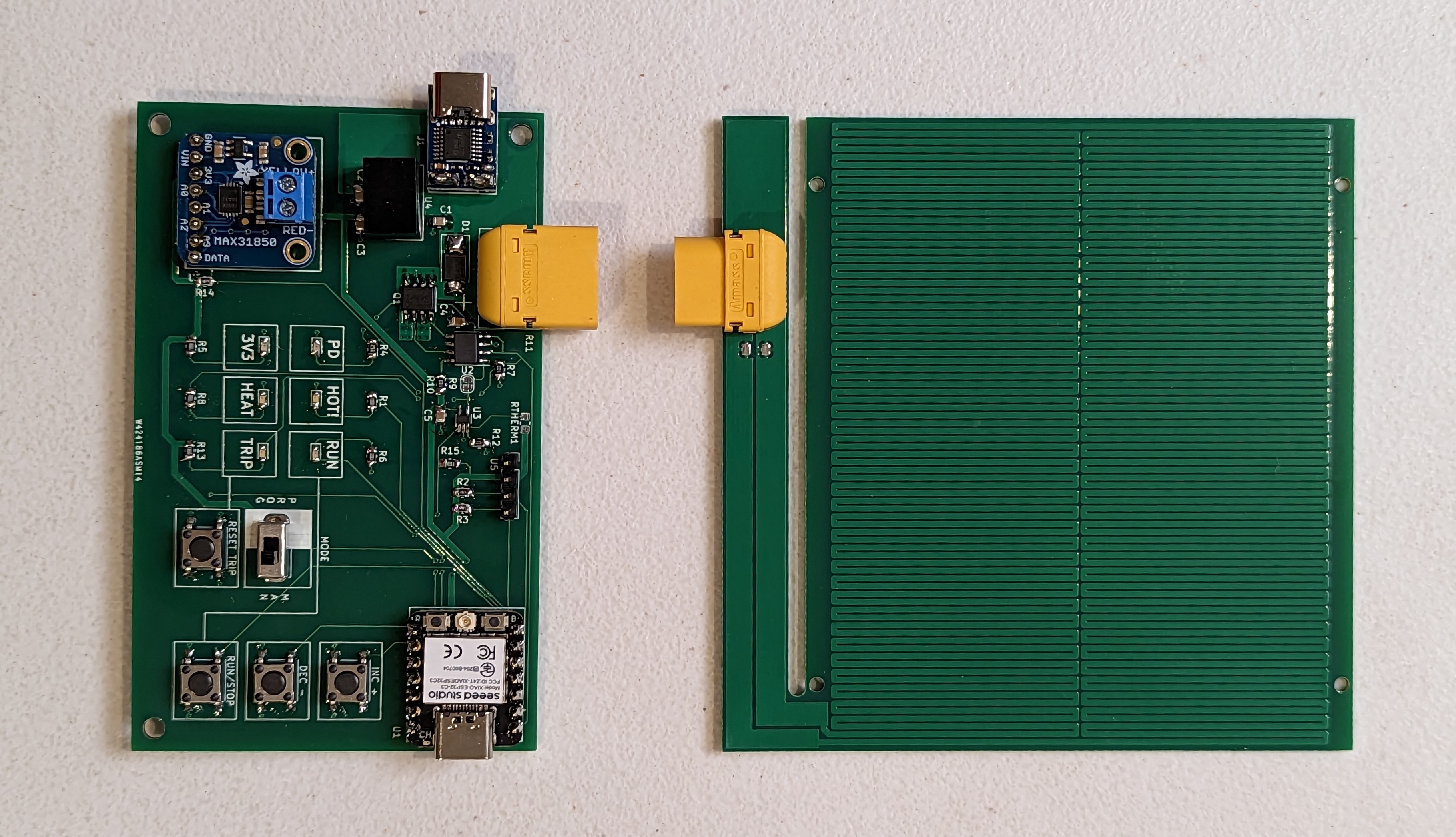
Here is the architecture I came up with:
There are two usb C connections- one for programming the micro, and one for power, equipped with a USB PD “trigger” chip. My new favorite controller, the ESP32-C3 is in charge of the show (and native USB C). A single thermocouple is used for feedback, and an RTD is used as a safety cutoff- basically if it goes above some target temperature, the micro will no longer be able to drive the power FET. This won’t prevent the board from getting super hot, but it does provide a hardware safety against exceeding some set temperature if the controller spaces out…assuming the thermistor does not fall off.
Additionally there are indicators for PD power, DATA power, data transmission (heartbeat), heater power, and safety over temp, hot surface, mode, and (finally) a temperature readout. These are diagnostically useful, and they should satisfy my desire for a cool looking annunciator panel.
One annoying thing is that the ESP needs to be driven at 3v3 while the rest of the stuff is happy at 20V. While a cheap, integrated buck would be a neat solution, an LDO is so much cheaper. I decided to go with the buck, since I wanted to avoid burning extra power when operating near the 100W limit of the power supply.
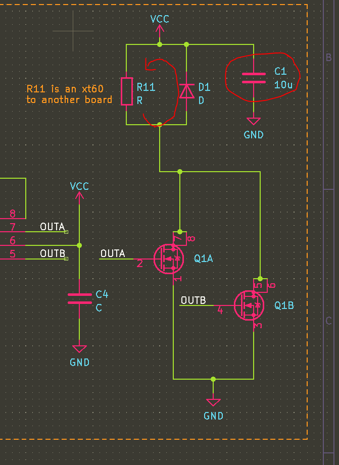
The heater itself will be driven by a gate driver like the NCP81071B, which is 20V tolerant. 20V will just barely allow us to use something like the AOSD32334C, which is a dual N FET. Paralleling the FETS will reduce the RDSon to almost nothing- close to 10 mOhms.
The heater element here is represented by a resistor and an inductor- I expect the trace to have some very real inductance (100s of nH?), which will cause a large voltage spike when the FET turns off. This could easily exceed the 30VDS of the FET, and cause it to break down. The flyback diode will hopefully prevent this. Additionally, a capacitor Cbulk will be chosen to prevent over-drawing current from the power supply. At 20V, the 3.3 ohm heater will draw 6A, while the maximum allowed current is 5A. By PWMing this, the average current will be below or at 5A, but when the heater is on that current needs to come from somewhere- the bulk capacitance C.
To connect to the heater itself, I am using an XT60 connector. These are low-resistance and they seem easy to get, due to their use in drones.
Safety + Temperature Monitoring
There are a lot of ways making a big heater that is capable of destroying itself can go wrong. Ultimately this device falls under the category of things you should unplug if its not in use, and definitely not something to leave running unattended. However there are a few details I added as a nod to safety.
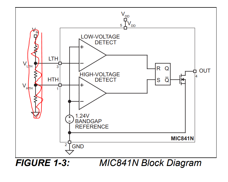
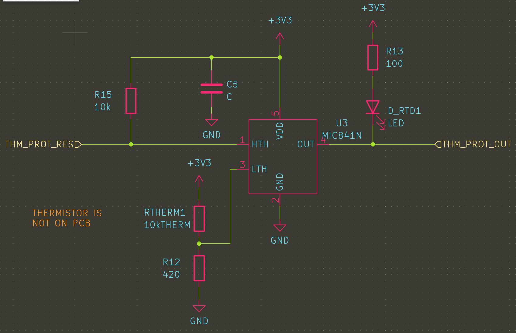
The first is a thermal trip based on the MIC841N The HTH input is fed by a NTC resistor divider that exceeds the 1.24V reference at about 200C. This SETs the latch, so the inverting output goes low, pulling down the enable pin of the fet driver. This is the case until either the whole circuit is reset (and the thermistor has cooled off) or until the reset line is pulled down by a button. Resetting while hot should result in an illegal state where ~Q is still 0.
Note: this circuit totally fails if Rtherm is removed, and it wont work if Rtherm gets disconnected from “the hot part”. If I wanted to add more logic, this could be resolved, e.g. inverting the logic of the resistor bridge. However, this is currently just a secondary protection. If it works nicely it can be refined later.
Temperature monitoring (for feedback and control) will be done with a thermistor dropped either onto the heater, or onto the target PCB. This allows for point control, near the stuff that you care about. For the time being, this will be made out of a MAX31850 thermocouple breakout that I have lying around from years ago.
Next Steps
With the heater and the controller designed, its time to get them made and then patiently wait for them to arrive!
I have started seeing a whole bunch of PCB hot plate builds, of varying success. I kind of want one now, since they seem very practical for one-off small PCBs, and most off the shelf solutions are quite large. However, I also want to improve on the state of the art of PCB heaters. These are useful for all kinds of stuff, from PCR machines to 3d printer hot plates.
There are a lot of challenges to overcome to make something that does not suck. Ideally, it could even be USB powered. Below are some calculations and considerations for making a pcb hot plate. You can see the WIP (scripts, pcbs, etc) on github.
PCBs are not a good material:
Using a PCB as a heater is not a new idea- however, in some ways, they are not good material candidates for high soldering temperatures:
The board will be at/above TG for a long time
solder mask/silk can discolor
could de-solder itself/the controller
repeated stress on copper tracks from board warping while heating
That said, several people have made them and they seem super-good-enough for this process.
Thermal Expansion
A lot of people worry about thermal expansion with pcb heaters- it makes sense because at the length and temperature scales that the heater will experience (100s mm, 200 C), real growth/shrinkage of the pcb will happen. With those temperatures and lengths, a FR-4 PCB will grow about .28 mm! An aluminum one will grow even more- .4mm! copper has a similar coefficient of linear expansion (alpha) as FR4, which means that the copper will need to stretch about .1mm/100mm of length. That is a strain of about .1%. That should be in the plastic deformation range for copper according to some stress strain curves I found, but it could cause cracking in more rigid parts of the assembly.
To further mitigate any expansion issues, I meandered the heaters on both sides, which should hopefully prevent pulling “straight” on any piece of copper. hopefully having a longer track (albeit, glued to the substrate) will help distribute the strain along the track- in the same way that a meandered track in a strain gauge rosette works.
In addition, I cut a slot between the hot part and the cold part, and put the connector thermally far away from the heater, while adding a lot of area for cooling. This should keep the connector from desoldering.
Low Voltage Efficiency Challenges:
A lot of these builds use lowish DC voltages to power the plate. This is not a great idea, because these things take a good chunk of power. Since the voltage is low, this drives up the current in order to deliver enough power. This results in losses in all the cables and connectors between the power supply and the heater.
As the impedance of your load approaches the impedance of the source of power, the power supply starts to eat a lot of power. I am considering all parasitic resistances here to be part of the “source” driving just the heating coil.
n is efficiency- as Rload gets to be about the same as Rsource, the efficiency will be about 50%- that means 50% of the power is going to get burned in whatever is supplying the power. This means that the rest of the circuit- connectors, fets, etc. need to be very low impedance compared to the load.
For example- to get a 100W heater at 12V, the Rload needs to be about 1.2 ohms This means that even a 100mOhm RDSon will drop the efficiency about 8%!
What would be ideal would to have the Rload to be greater than the R of everything else, by a lot. This is possible, but it comes with a catch- the current will be lower, and therefore, the power delivered to the heater will be low. Lets compare two cases, RL = 1 and RL=9, for Rs=1, and a source voltage of 10V that can output up to 5A.
Case
n, efficiency
Current (A)
Ptotal
Pheater
RL = 1
50%
5
50W
25W
RL = 9
90%
1
10W
9 W
An interesting (and not very important) aside is that for a particular heater power, and an infinitely powerful supply, there are usually two operating points for a given heater power. Check this out:
This gets turned into a very ulgy polynomial:
Lets look at a case where we claim Rsource = .5 ohms, V = 24v, Pload = 80 w.
If you crank this through the quadratic equation, (with some rounding) you will get R load of about 6 or .04 ohms. two very different resistances, but if you look at the same table you will see:
Case
n, efficiency
Current (A)
Ptotal
Pheater
RL= 6
92%
3.7
88W
80
RL = .04
7%
44A
1000W
80
yes- I rounded a lot but this is about right
Obviously, a heater with .04 ohms of resistance is impractical – the heater would be tiny (since the resistance has to be low), it would get SUPER hot because of the low thermal mass, and we would need to draw a kilowatt to use it.
Low Voltage Workarounds:
The good news is that the voltage does not need to be very high. Even a voltage of about 20-24 V (commonly available) is much better at delivering power than 12v.
Boosting to a higher voltage can help too. This won’t help as much as not having a low voltage at all, because the loss in the wiring/connectors in the low voltage section will still exist. However it could give more flexibility in the design or choice of heater elements. e.g. a 12W element that runs at 12V will have a resistance of 12 ohms (and a current of 1A). running this at 24V will result in a quadrupling of output power to 48W.
Ok, how much power do we need?
If we look at the existing hot plate examples, one figure of merit seems to be the steady state temperature at a given input voltage, and therefore power. My suspicion remains that connectors are eating a lot of power here, because the numbers do not add up. For example, at 3:10 in the hot plate V2 video we see the power supply is at 12V 7A, for a total input power of 84W. The temperature is 196C, with a room temp of about 25C. The heater diameter is .01 m2.
If the temperature is stable, that tells us energy in = energy out:
Using these numbers to back-solve for h, the convection coefficient, gives us about 44W/(m2k), which seems high. Given a similar delta T and the 70*50 area of the after earth board, the coefficient is about 10 W/m2k. These numbers seem high- I do not think all this power is getting delivered to the board, since a typical number for h is closer to 10-20 W/m2k for a pcb application. Its possible I am missing a few mm2 of area, or a lot of radiation or conduction, but these pcbs seem reasonably thermally isolated and appear to be in still air.
These designs come out to 5-10W/in2, or about 10kW/m2. I have seen a lot of heaters that claim to be 5-10W/in2, so that seems like a reasonable power to target.
Doing the math forwards (delta T of 175k, A= .01m2, h=25W/m2k), gives a desired wattage of 44W. I will aim to overshoot that, because it will reduce the heat-up time.
How fast does it need to get hot?
A good rate seems to be about 3C/sec, based on some reflow profiles. however, this rate needs to be done not only at the lower temperature, but near the top end of the reflow temperature- lets say 200c. This is important because if the heater is designed so that the max temperature is the reflow temperature, the heating rate will be slow as it approaches the max temp asymptotically.
drawing of typical newtonian heating
This is semi easy to estimate- we can make some assumptions, like that our heater is infinitely thin, massless, and is heating a plate that it is in very good contact with. the plate is also thin, so we don’t care about the gradient across it.
This basically says Temperature is equal to thermal mass * energy in an object. Taking the derivative with respect to time gives us a heating rate that depends on the heat into/out of the object. If we assume mostly convective cooling, and choose Qin, we can get a rate of temperature change. The delta T chosen tells us what the rate will be at a given temperature above ambient.
assuming a 1mm aluminum platen, with .01m2 of area, the volume is 1e-5 m3. with a density of 2.7e3 kg/m3, and a specific heat of 900 j/kgk, the platen has a thermal mass of about 73j/k.
for h=25 w/m2k a= .01 m2 dt=175, the convection term comes out to 43.75W (this is the same as the power needed to heat to this dt)
Tdot should be 3c/s,
so solving for Qin gives an power (at the heater) of about 100W. This is a rough SWAG, and it comes with the caveat that it will likely be even slower than that, due to delays in conducting that heat to the PCB.
Using USB C PD:
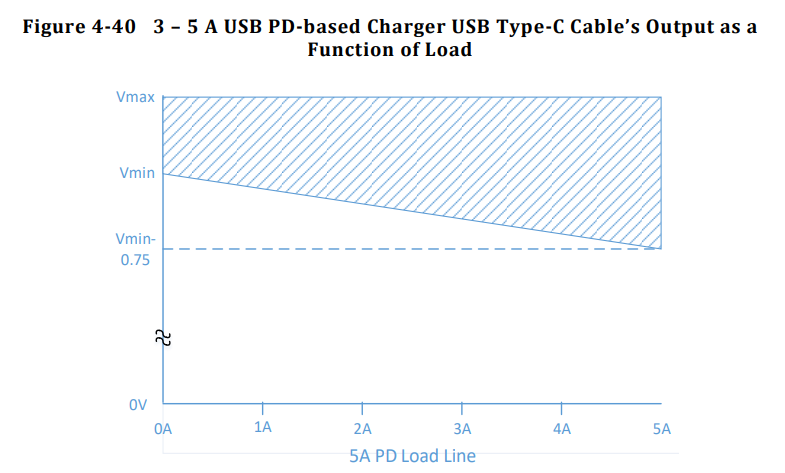
A USB C power delivery brick can, in theory, supply 100W. Really getting 100W out of a USB PD charger seems to be a bit of a stretch. There are tolerances on the actual voltage a given supply must provide, plus an allowable voltage drop (and power loss) in a to-spec USB C cable. Per the usb C R2.0 spec:
This Vmax and Vmin represent +/-5% of the allowable voltage. At 0A, there is no drop on the cable, but at 5A there is an allowable 750 mV drop. Interestingly, this drop is not symmetrical- only a 250 mV drop is allowed on the ground connection (even though it should have the same current flowing through it). This voltage drop at 5A means that a USB cable is allowed to burn about 3.75W.
This means the worst case voltage to come out of a 100W PD supply and cable at 5A is really 18.25 V, which is really closer to 91W. However, as much as 20.25V can be delivered at 5A, for 101.25W (with an ideal 0 ohm cable).
This means to get the full power out of the lower allowable voltage chargers, (18.25V), the heater resistance will need to be 3.65 ohms. however, that will draw too much current on the high side. the solution seems to be to cater to the lowest voltage, and then PWM the heater (which I will do anyway) so that it does not exceed the average current draw for higher voltage/lower resistance supplies. Designing around the higher voltage supplies will result in a under-powered design, since we will not get the full 5A at lower resistances.
Additionally, there needs to be some allowance for other resistive circuit elements, e.g. the switching FET, solder joints etc. Estimating a few 300 milliohms for those seems ok, so so the real target heater resistance should be about 3.3 ohms at room temperature.
Resistance Temperature Sensitivity:
Resistance of materials increases with temperature. Copper increases about .0039 ohms per degree ohm. With a delta T of 175K, and a target resistance of 3.3 ohms, this means that the resistance will increase by 2.2 ohms! This means that at higher temperatures the maximum output will be closer to 72W.
It is easy to calculate what original resistance would give us 3.3 ohms at 200C- this turns out to be about 2 ohms. However, the bulk capacitance required to smooth out the ripple at 10kHz is about 1000uF, which is expensive to implement. Using an electrolytic capacitors incurs a pretty steep power loss in parasitic resistance, and ceramic capacitors are too expensive for the design. I will stick with 3.3 ohms for the design, and just loose some power generation at higher temperatures.
Heater Design Math:
What follows is a detailed design of the heater traces. An important concept is sheet resistance- this is the concept that the resistance of any square of material in a homogeneous sheet has the same resistance. 1 oz copper has a sheet resistance of about .5 mOhms, per square.
As we know from our previous calculations, the resistance of the heater should be about 3.3 ohms. We can use this equation to get the number of squares:
From this I calculated that the number of squares needed is 6600. This means the trace for the heater (if its made of 1 oz copper) to be 6600x longer than the width.
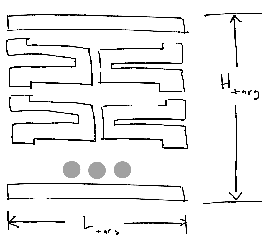
I want the heater to be about 100×100 mm, or less. This will give us an area of about .01m2, which was used in the calculations above for heat transfer. Ideally, the heater would be a little smaller, in order to hedge on the side of performance. Another practical consideration is putting the power terminals next to each other- this will minimize the length change between them when hot, and it will make the wires going to the heater short (preventing a wire run from another edge or corner of the board).
In order to meet these requirements, I wanted a rectangular pattern that would fill in the heater rectangle. I opted for what I decided would be called a double zig-zag, which can be cut anywhere on the perimeter so that the power terminals are next to each other. The extra long trace should also help prevent from stretching the copper under thermal expansion, since the whole pattern should act like a spring.
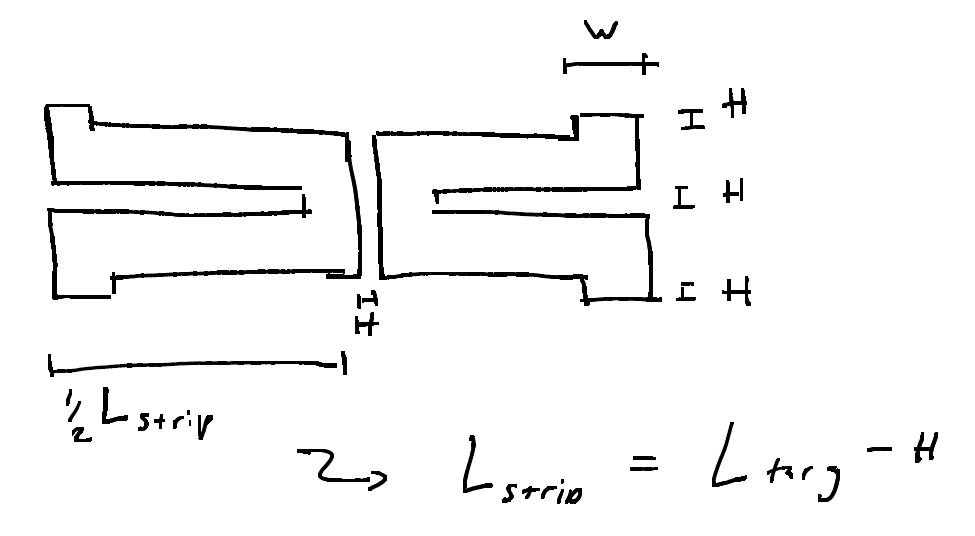
This drawing shows the units broken down- two long bars Ltarg long of width W, and several units that would each be connected to each other. Each unit has these dimensions:
The ideal distance between the tracks, H, should be very small, because it will result in more coverage of the board in heater tracks, and therefore more even heating. I chose to start H at about 6 mil/.16mm. H needs to be varied so that the total number of units, N, is an integer. having a half-unit means that the spacing will be off or that it will not be possible to terminate the pattern properly. The next thing to do is to come up with a couple relationships for the geometry of the pattern. The first is that the pattern must be a certain number of squares long. This sum is the top and bottom width full length bars plus N units * squares per unit. The Number of units, N, also has to be equal to the target height of the units (Htarg – 2w) divided by the unit height. Here h is the spacing between units, and H is Htarget.
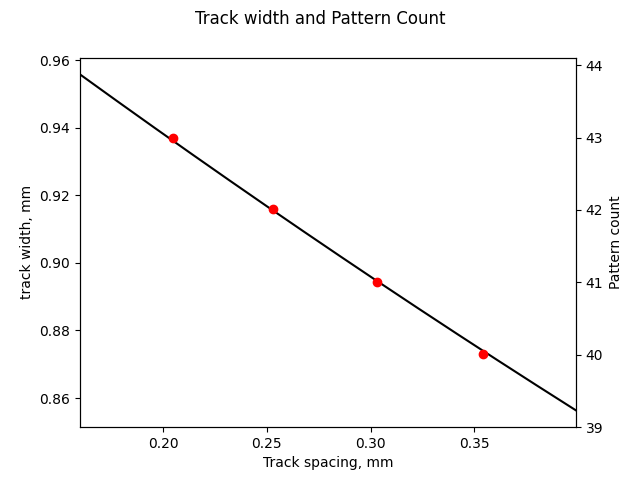
These first two expressions combine, after some work, into this ugly polynomial. we can now input an h, spacing between traces, and get out w. w allows for computation of N, the total number of units, which must be an integer to be valid. see plot below to compare red dots (N) to track width (mm) vs spacing, h (mm), as the spacing is increased.
With this computed, it is easy to choose the best outcome, where the track thickness is maximized, and spacing is minimized, to create an evenly heated area.
Final design:
I decided that the heater dimension should be 100×76, since it is a little smaller than .01m2, which should give better performance at 100W. It is also a reasonable size for most PCBs I would make and under the price break dimensions for aluminum PCB.
Since the pattern can’t go all the way to the edge, and because the mounting is somewhat TBD, I decided to subtract a 1mm border on the long (100mm) dimension and add 4mm border on the short dimension. This makes the final dimensions for the board 100×100 (including connector), and the pattern dimensions 98×78 mm.
For a target track resistance of 3.3 ohms, the calculator reports that the width should be .996 mm, with .267 mm spacing, and 38 repeats.
Kicad Plugin
Of course drawing this trace is tedious and difficult to get right. A plugin was designed to draw the trace meander. Details can be found on git.
Next Steps:
The next thing to do is to ship the design off to be fabbed. I’m planning on trying both FR4 and aluminum substrate PCBs. FR4 has the advantage of having a similar linear expansion coefficient as copper, and being an ok insulator. Aluminum on the other hand, is possibly more rigid than FR4, and is a good conductor/heat spreader- this would be good to prevent heat buildup in any one trace. I will also need a controller for the heater, with a micro, a sensor for feedback, etc (post coming soon).
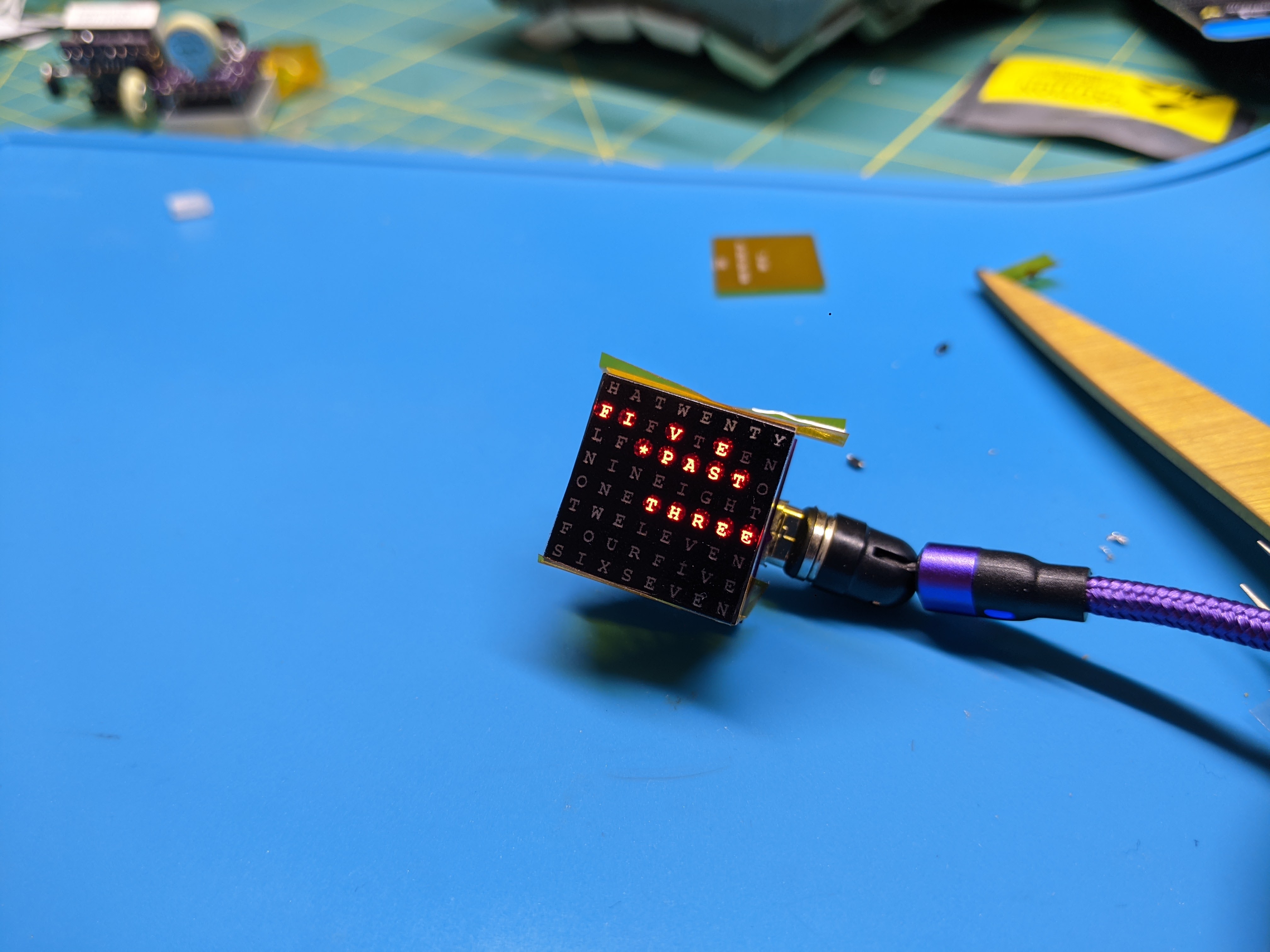
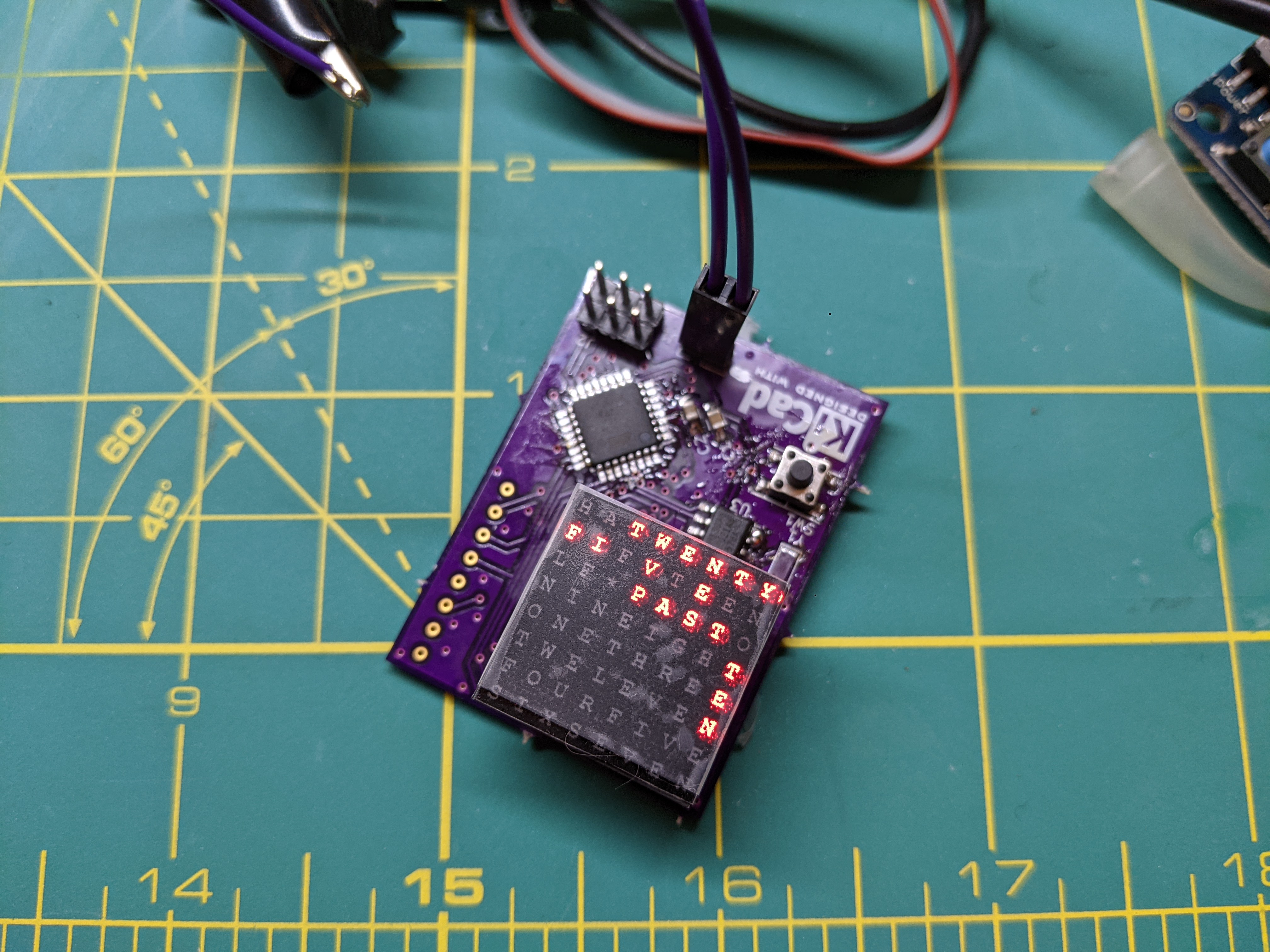
Just another version of the micro word clock. Like the old version, this uses a matrix that is more widely available than the original matrix, including on adafruit. Unlike the older version, this version is very tiny (no larger than the display) and it incorporates a battery fallback for the RTC, as well as a USB connector for power. This was a fun layout as I had to balance my hype for assembling teeny tiny parts (generally low) vs size.
PCB Layout Trickery
there wasn’t a lot of real estate on this board once the display was placed, since it is through hole. The pins basically cage in the rest of the components. In order to get a clean layout (no vias on any of the display pins), I did a lot of pin swapping. Based on having to tweak the code last time for a new matrix, I knew that I had total flexibility here.
I also had to add a programming header somewhere but I really had no room on the front or back for even something like a tag connect. My solution was to add a connector via a castellated connector on the edge of the board. Then I used pogo pins and a little jig to make a bed of nails so the boards could be reprogrammed once assembled.
I also used a magnetic USB connector, which is ancient Greek for “an accident waiting to happen”. These cables come with a microUSB to tiny PCB adapter, and the cable itself snaps on and catches the adapter. the “hot” side has absolutely no protection that I can see, and actively accumulates magnetic (conductive) particles. The power is also routed through an open joint on the end of the connector (kind of a slip ring system). Since it basically adds two unreliable, moving slip joints to the power path, its very important for the coin cell to do its job to prevent the RTC from losing time.
Next Stop:
I think the next stop for this project is to teach a few people how to use kicad. its a cool little project that’s hard to mess up, but that makes a pretty neat little widget without too much trick soldering.
I am planning on teaching some people to use kicad, since its my new favorite EDA tool. I searched high and low for a decent circuit that would do something cool, with a good variety (but small number) of parts. Basically something fun and not intimidating. I got hooked on formatc1702’s micro word clock. It is an excellent use of the atmega8 series unusually high current drive outputs.
Challenges
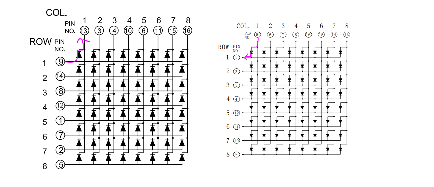
left- original gyxm-778 matrix. Right adafruits luckylight KWM-20882CVB matrix
The one catch was that I had a lot of trouble finding the GYXM-788ASR LED matrix called for in the bill of materials. Fortunately adafruit sells a similar 8×8 matrix from luckylight. I tried to design around this by including both footprints, but I ended up mostly making a mess (and I still couldn’t find the 788!). Both are common cathode but the row/column nomenclature is flipped. To formatc’s credit, they did a good job with the firmware. It was easy to find pindefs.h, which let me swap around pins until I was happy. My strategy was to create a test pattern and make sure it shows up where you want it on the matrix. This was much faster than tracing every signal and creating the right pin definition the first time.
The second catch was that after programming, I couldn’t get the time to change! After glossing over the code it seemed like this must have something to do with the RTC- and after some gentle probing/touching the board it would occasionally work. Initially I attributed this to the crystal not starting up, but after many power cycles and other pokes, it seemed like the crystal would actually run just fine. As a last resort I read the datasheet, and lo and behold, the Vbat pin needed to be grounded.
I bridged these two pins
A blob of solder quickly remedied this deficiency in my pcb, and afterwards changing the time worked just fine. I suspect that sometimes the chip “just works” if that pad happens to be at the right potential on reset, but sometimes it doesn’t. The button presses update the RTC time, not a time on the micro. So if the RTC does not start up, then you can’t change the time.
Other Notes
Pin1…probably. I prefer a dot!
I used the default footprints from kicad for a lot of the parts, and the pin 1 designators are a little wishy-washy. They look more like an printing error than a clear indicator for pin 1. I guess I will get used to it instead of re-creating every part from scratch, but if I only have a few parts, throwing a dot on the PCB would go a long way during assembly.
I should have also added a polarity marking on the power connector, and a couple of i2c test points wouldnt have hurt either. Since this was a quick board just for me and the parts are big, I didn’t worry about it.
Upgrades for V2
I figured if I was going to do this board again, I may as well overdo it. I managed to cram everything into a board roughly the same size as the matrix itself, even after I added a coin cell and a USB connector for 5V power. The coin cell will keep the RTC running for about 10 years, even if it loses usb power. This way I can program it, ship it to someone, and they can just plug it in and the RTC will know what time it is. The ground plane is far from perfect but its about as good as I will get with a board this size
Since the time will basically never need resetting, the switch for changing the time is very very small. I used the NanoT switch which is about the same size as an 0805, which is very very small indeed. And because programming is now a one-time affair, I moved the programming header to castellated vias/PTH on the edge of the board. They .1″ pitch so they should be easy to solder to headers if I cant scare up a pogo pin jig for them. For some reason the ground pad shows an air wire. The 5V is purposely left floating since I don’t care about that connection.
Documentation
The git repo can be found here. Its probably not ready for prime time yet, but check the readme. I will update that when its reproducible.
I am building a one handed chorded keyboard, which is exactly what it sounds like. It is a keyboard, but instead of using the qwerty layout, it uses chords of keys as input.
The main reason I want to build a one handed chorded keyboard is because it would be convenient. A few of the advantages I see are that it will be smaller, cheaper, and will reduce the amount of devices that I use to interact with my computer.
Lets look at a typical interaction with my laptop, which is my primary computer (my other computer is my phone). I have 6 input devices to choose from. They are:
built-in trackpad
built-in nub mouse
built in nub mouse keys
built in trackpad mouse keys
tray-style keyboard
logitech mouse (wireless)
my laptop interface
This is already looking bad. First off, there is a triple redundancy in the pointer category. second, the nub is useless as a normal pointer, because its left button is underneath my left thumb when my left hand is on the home row. the nub mouse buttons are also extra-super-hard to push, so you don’t accidentally push them with your thumb. The trackpad has a similar problem in that it is crammed in there near the spacebar, and sometimes it gets pressed by my thumb and does weird stuff. To add insult to injury, the keys are huge dust collectors, and can jam if they get a big enough piece of stuff in there, which happens frequently with little pieces of 26 gauge wire insulation which is just big enough to slip into the gaps.
On the other hand, the logitech mouse is a joy to use, provided you have a large flat surface to work on. However, I prefer the logitech trackball mouse (m570), because you don’t need to move it at all and it is larger and more comfortable for my hand. That said, the build quality of the m570 is sub par, and it feels kind of cheap-o.
So lets look at a pretty common workflow for solidworks. I start out left hand on the keyboard, right hand on the mouse. Thats great for clicking around, but eventually I need to enter a number. Then the dreaded top-row numbers come into play. lets say I need to enter “23.43”. The “.” button is way over by my right hand, with the arrow keys, enter, and backspace. So in order to enter something, I have to move my left hand across my body to those keys, which my left hand does not normally type on. So instead, I end up moving my right hand to the keyboard, and then back to the mouse, and back and forth, and there are numkeys, and shifts and lot of moving. it is particularly annoying because I need to do this over and over again in my workflow.
Now lets think about writing code. Alpha characters are pretty awesome on the querty layout, but { } [ ] | : ; ” ‘ ( ) = + -* all require a lot of right-hand movement, and a lot of them involve holding down shift. While this has become second nature to me now, I would gladly swap a few alpha characters for those keys. Or even have a querty[]{};:'” keyboard, with more keys! QUERTY was designed for typists on typewriters, not computers.
Crazy busy desk. This is a real picture of what my desk looks like.
This is my final whiney paragraph for this post, but take a look at this picture. This is a real, in-use picture of my desk. Look how many keyboards are on this desk. There are THREE. two laptops, and an external keyboard because the netbook kb is too small, and too far away, but there is barely room for the external keyboard because of all the crap! To mouse on either of these machines is also a pain, and it means I have my wrist unsupported on the right, or I have to reach over a tangle of wires on the left. On top of it all, I was barely even using the computers- they were mainly just for datasheets or running scripts.
With a chorded keyboard, I will be able to put my laptop veeeery far away and control everything through a chorded keyboard and mouse combo. Even if the keyboard is utterly crappy, and can only type 2 wpm, it will be plenty good for looking at datasheets, or goggling something while I am at the bench.
For schematics and code, check out the revobots page here. For video of the bot, look here.
Well folks, it is about time I wrapped up REVOBots, which turned out to be just as much work as expected; which is to say that it took more time and effort that I had planned. And as expected, attendance dropped off towards the end of the semester as our project based classes go into full swing and spring (and the opportunity to lounge around outside) starts to warm up the weather.
REVOBots 5 ended up being an explanation about some code that I wrote, and an introduction to EagleCAD. I have attached the code to the revobots 6 pdf because if fits in better there.
A student testing a ‘bot in the dark
REVOBots 6 was a build day dedicated to making the revobots go. There were two critical failures on my part before revobots 6:
Did not spec out the motors/H-bridges properly. The motors turn out to run at 3V, while the H bridges run at 5- ~30 V.
Did not order parts early enough
That said, the bots still work at 5 volts, albeit with a drastically shorter motor life. But operating at 5V this seemed to cause too much of a current drain on the power supply, so we got some weird twitchy behavior during the class. Since then I have developed a cheap fix using two 2n3906 NPN transistors, and a smattering of decoupling caps.
Top view of the ‘bot
What is a decoupling cap though? Doesen’t the five dollar arduino already have them?
The answer to the second question is yes, but the cap was not big enough. The problem the circuit was having was that the batteries were trying to output a constant voltage. This means that as current demands changed in the circuit, the battery had to adjust the output current. With the microcontroller taking only a few miliamps, the circuit is not drawing much power. BAM! Motor turns on and what happens? The battery needs to supply more current, but can’t. Then the mcu shuts down as it looses power, sending a short pulse to the motor. So bigger decoupling caps were needed to smooth out the power supply, which the caps do by charging up to 5V, and then discharging if the voltage drops due to sudden current demand.
So the symptoms were: mcu turning on and off, which I could tell because the status LED I had attached was flickering.
The prescribed cure was: Find all the capacitors on my floor, and stick them across the power rails.
Result: REVOBot works! Check it out here! (In this video it is running away from light because I have the motors running in reverse).
So the other day I got bored and prototyped something which I quite liked for revobots. It might be to people advantage to see it here before revobots meets again in two weeks, so I thought I would do a post.
One might wonder what a manual robot is. Well, thats what I am calling this. It doesn’t have any actuators, so you have to move it around with your hand, but if you follow the instructions it gives you (via the LEDs) it will follow a line!
The pseudoalgorithm for this is that each sensor has some threshold so that it reports a status back- either light or dark. If the middle sensor is dark, and the outer sensors are light, then light no LEDs. If any sensor is not on the proper darkness, a corresponding LED is lit. So if the left sensor strays onto the line, and the other two are off the line, then the middle and left sensor LEDs turn on, indicating the need for a right turn.
Oh no! Hard to port!
Soon I will have this mounted on a revobot chassis with power, then I will post a video and documentation!