Reading a thermistor seems like a pretty straightforward task, and there are a lot of guides on how to do it, either using just the beta value, or using the full set of coefficients for the Steinhart-Hart equation. I wanted and needed to do something a little different, because I wanted to measure temperatures somewhat accurately over a wide range (25-200C) with a single thermistor, for an upgraded version of the PCB hotplate.
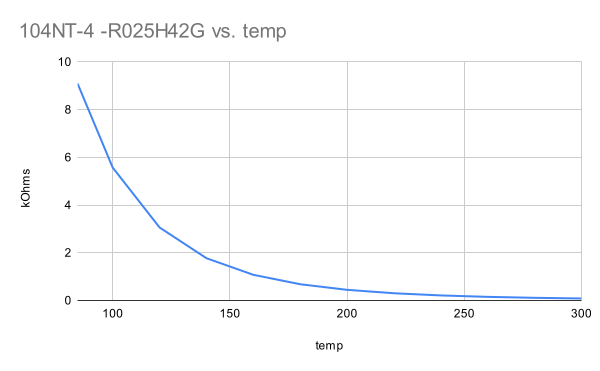
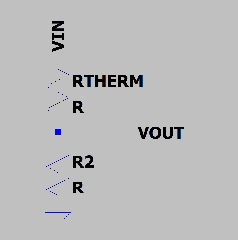
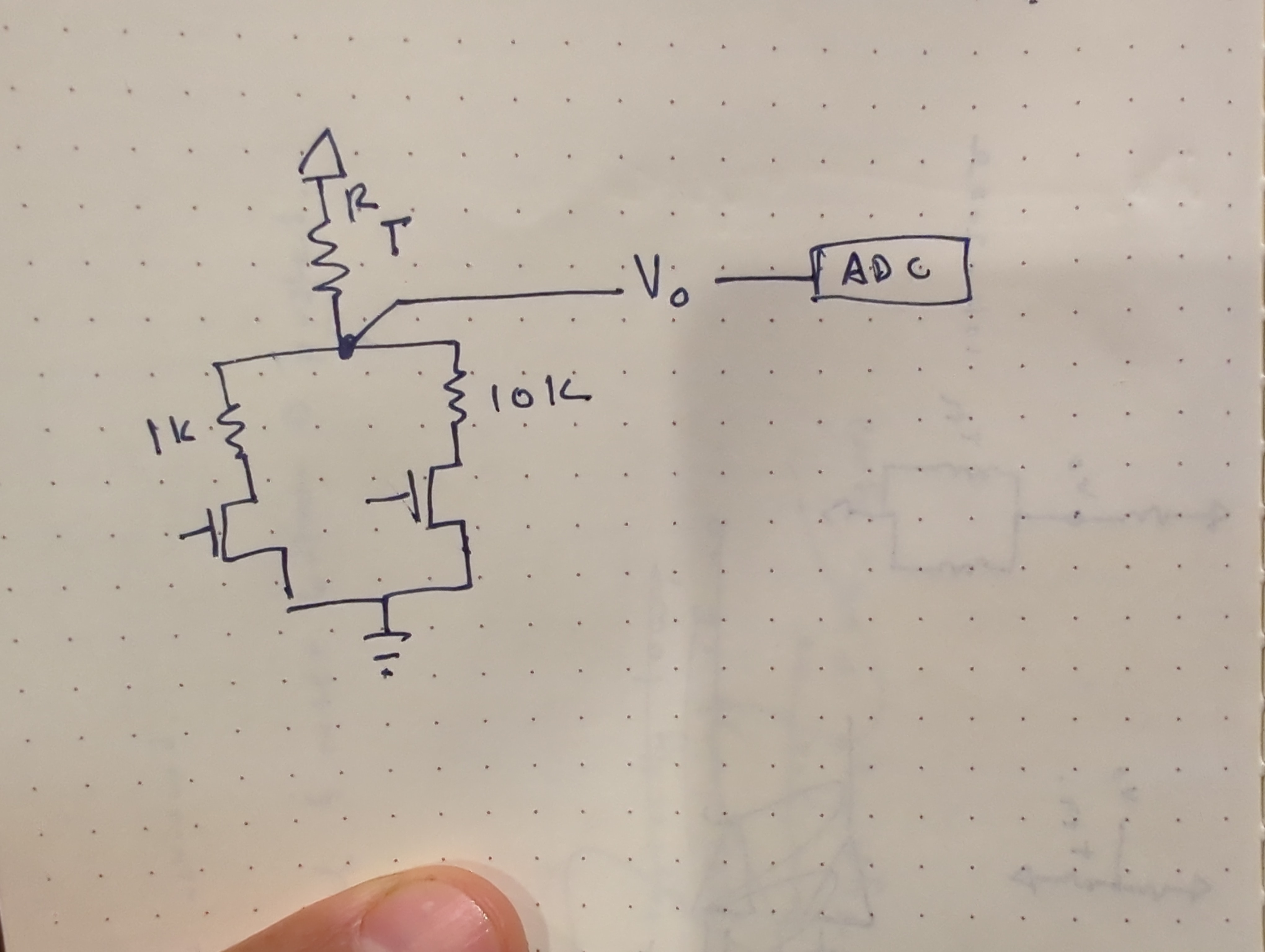
Measuring this range is difficult because the resistance of the thermistor changes a lot over the range I care about. at 25C, this particular model is 100k ohms, and at 200C it is about 1k ohms. It is very not linear, changing very rapidly at first. Thermistors are often used in a voltage divider, where the output voltage is related to the temperature of the thermistor:
This causes a problems for my implementation because choosing other resistor in the divider causes the most sensitivity near the value where Rt=R2. That is, the temperature sensing will be easiest near where the thermistor and the other divider resistor have the same value.
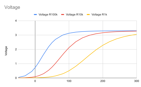
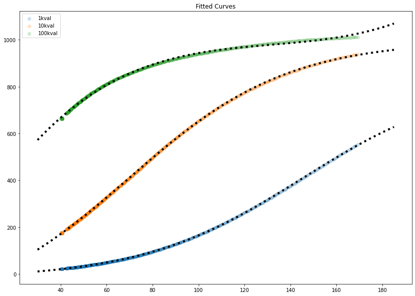
This is a chart showing the expected output of a voltage divider with three different resistor values, computed from the temperature-resistance chart plotted above. The steeper the curve, the better, since a small change in temperature will create an easily measurable output. But none of these curves are linear across the whole range that I care about, from 25-200C. Instead, the 100k looks good from 0-50C the 10k looks good from 50-120 and the 1k looks good from 120-200. At the center of each of these ranges is where Rt=R2, and the output of the voltage divider is about half the input voltage.
My solution was to use several different resistor dividers instead of a single resistor divider. The final implementation uses an analog mux instead of discrete FETS, and included a 100k resistor divider as well.
Calibration
While it would be possible, through first principles and careful measurement, to figure out some mega-equation for all these components, I decided it would be a lot easier to write a script to calibrate each “channel” of the measurement. These thermistors are calibrated against a thermocouple, which was the original sensing element on the hotplate. To collect calibration data, I just measured the hotplate with the thermistor and thermocouple taped together. This produced the curves above, as expected from the simple simulation. Shown in black dots are fitted curves- the bottom two fit a sigmoid/logistic curve, and the top one (which didn’t have enough data to fit to a logistic curve easily) is fit to a 4th order polynomial. The 100k resistor values (green, top line) were pretty useless above 40C, quickly flattening out.
These curves give us a value that predicts ADC ticks for an input of temperature. The inverse is really what we are after, but that is easy to do mathematically.
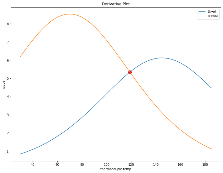
Looking at the two remaining 10k and 1k curves, the question is where to swap from one to the other. The goal is to keep the amount of ADC counts per degree C as high as possible over the whole range. This can be found by inspecting the derivatives of the fitted curves and finding where they meet (in this case, just around 120C).
This chart also shows why exactly a single value for R2 in the resistor divider would be bad. For example, below 40C, the 1k resistor shows less than 1 tick per degree C, so a 1 degree change would be hard to measure there.
Limitations
This was done with a single set of data, so it may not be accurate for all time. Taking more data in the future would be neat, especially because the python script for analyzing the data will just spit out numbers. It would be interesting to compare the calibration coefficients for various data sets to figure out how much they change, run to run. Hopefully it would be a small amount.
Solution Cost
The reason I didn’t go with a thermocouple is that the reader and the thermocouple alone would cost about $10 in parts. I usually buy multiple ICs per prototype (in case of an accident) which would cost something like $15-20 in parts. The parts for the equivalent thermistor solution cost about $2.50 per unit, which is cheaper than just the thermocouple reader IC.
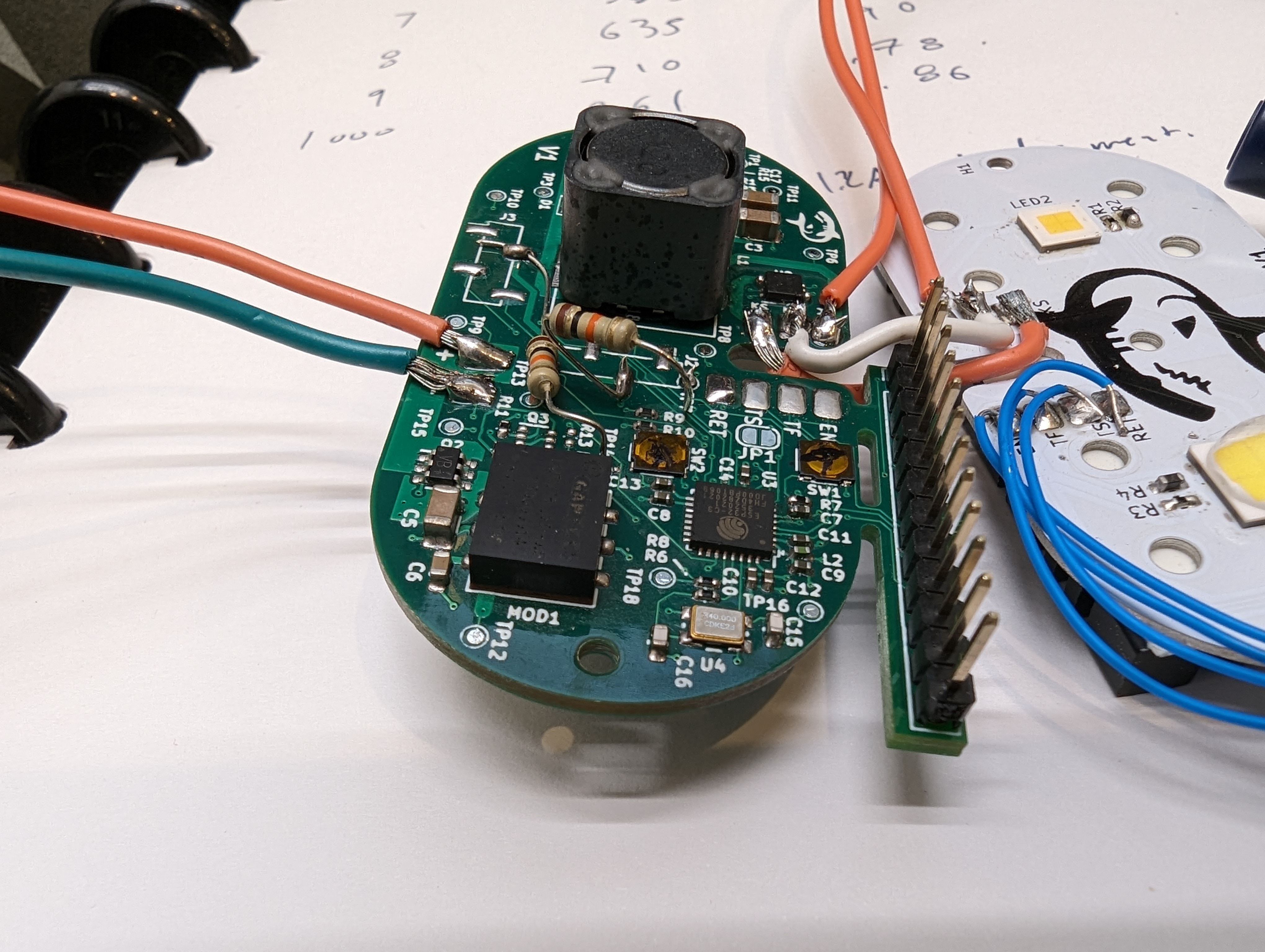
With the dive light parts in hand and assembled, it was time to test it out and fix all the inevitable mistakes. I expected this to go pretty well, and bringup for most low power functions was a breeze- however, at higher currents, this thing is a pretty good heater. This led to buying a fun tool – a thermal camera!
ESP32 bringup:
This was my first bare-chip-down ESP32 design, and it was actually pretty easy to do. I used the variant with internal flash to save room, so the only external components were a crystal + caps, some passives (R’s and C’s), and a switch for the RESET line, and a switch on the BOOT (gpio 9). However, there are two additional strapping pins (GPIO 0 and 2) that needed pulldowns. This was annoying since these pins were not pulled down on the pcb – some of them were pulled up, so the parts that did that needed to be removed, and the functionality of those circuits needs to be checked some other way.
I think in the future, it would make sense to avoid using the actual boot and reset buttons and use something like the ESP-PROG to toggle all the lines. Needing to push buttons to upload code is a drag!
pink=paste. This footprint has too much
I also consistently had issues soldering the QFN package the ESP comes in- I think this was due to too much paste on the center thermal pad. This causes the chip to float, and sometimes this causes one side of the chip (or a few pins) to lift. Next time I will reduce the amount of paste on the center pad to fix this, but I resolved it here by removing the chip, solder-wicking the thermal pad, and then re-soldering the part. Using low temp solder paste made this really easy.
LM3409 Driver bringup:
The LM3409 bringup went relatively well, but thermal issues started to crop up pretty much immediately. There are some surprising deficiencies in the layout and parts that I will be modifying for future revisions. The thermal camera really helped to visualize the issues quickly, and given the number of thermal/power projects I have worked on recently I am sure I will get to use it quite a bit.
PFET Gate Charge
One hair raising issue was that during bringup, the board started to smoke. This is almost always a bad sign. In my original estimation, this was caused by the buck PFET getting hot due to having a high gate charge. The odd thing is that the freewheel diode also got really hot, and stayed hot even if the led was very dim.
A very basic thermal investigation with two thermocouples showed that the FET was getting hotter than the diode, at least initially. However, I did smoke several diodes in the process.
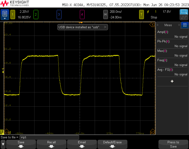
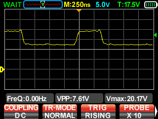
original fet gate voltage. roughly 200 ns of switching time.
Reducing the gate charge did appear to solve the problem, and there was even a note in the datasheet (that I glossed over) about keeping the gate charge below ~30nC. Having a high gate charge is problematic for two reasons- it keeps the FET in a high RDS region for longer during switching, and it requires more power from the gate driver on the LED controller, which also heats up. However, this was not the real problem.
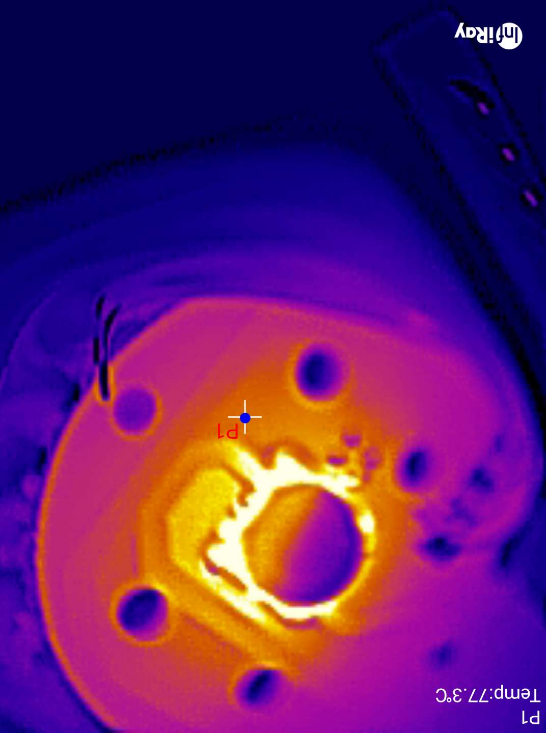
Overheating and Limp Mode:
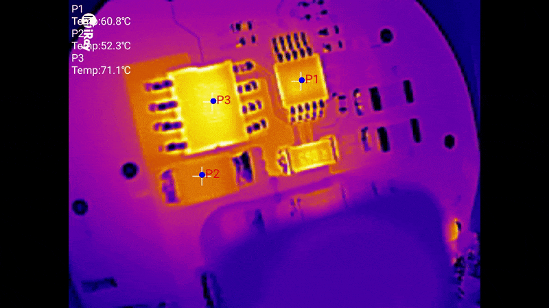
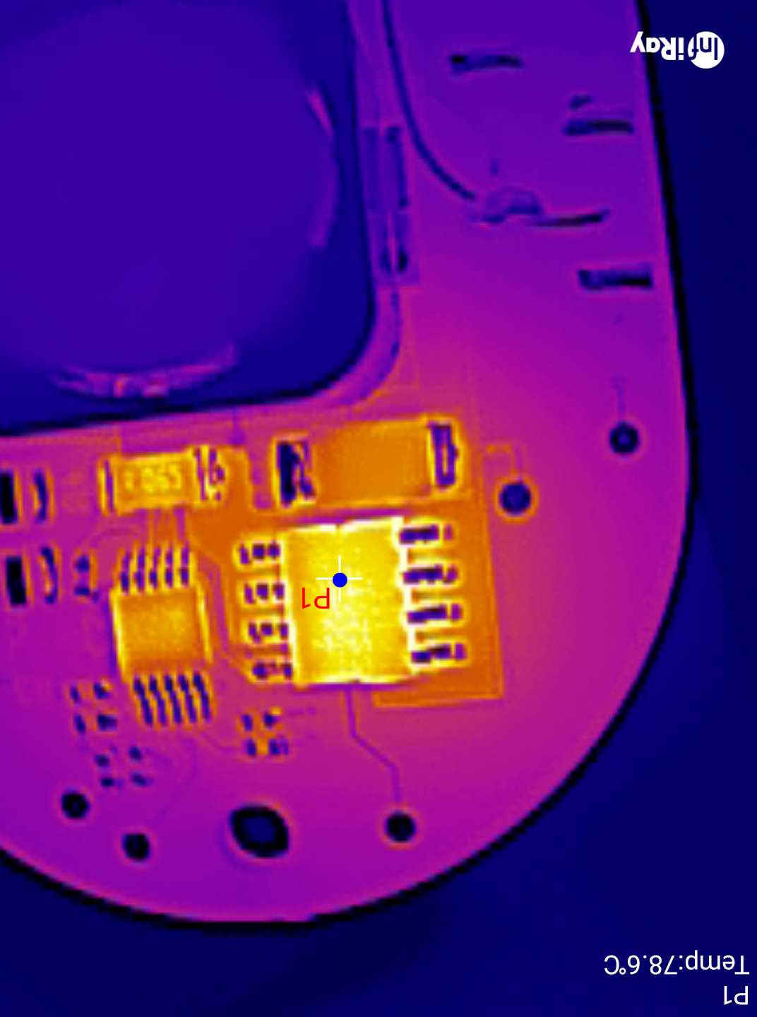
Note that initially P1, the driver heats up to ~70C. Once the driver gets hot, P2, the diode, gets VERY hot (150C!)
Gate charge was not the entire story. With the FET replaced with a lower gate charge/higher RDSon model, there was still an issue! With the LED aggressively cooled (to allow it to live), the device would still go into some kind of limp mode after a few minutes of operation at high currents (3.6A avg, 12V, about 42W).
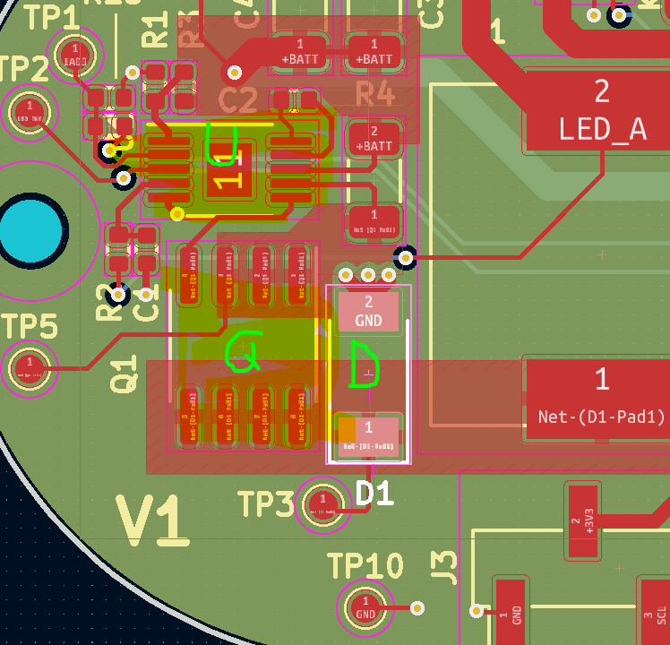
This seems to be due to the driver itself overheating, which is due to my poor thermal design. The driver is marked U in the layout above- this is supposed to have a thermal pad connected with vias to ground. I omitted the vias, essentially insulating the chip- no good.
Gate Voltage
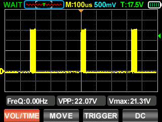
Second, at high currents, the regulator needs to switch frequently to keep in regulation. Estimating from the gate voltage above (in terms of time), and assuming maximum 1A gate drive currents, I estimate that the total switching time is at least 100nS with a period of about 1375nS. The average voltage is about 16.5V, so 16.5V*1A*D = ~1.2W. This would probably be easy do dissipate if I hadn’t insulated the chip. Reducing gate charge helped reduce the power this chip was dissipating, but it was not the root cause.
To make things worse, I didn’t add much copper to dissipate heat on the FET, and at least half the copper is on the side of the driver, which actually makes things worse (its easier to for the FET to heat the driver). Adding some vias to a large plane on the back, and increasing the area on the front will increase the area the heat can easily dissipate from.
The reason the diode gets hot is because usually, the diode only free wheels for a short amount of time- when the FET is off. When the driver goes into limp mode, it has to dissipate all the energy stored in the inductor, many times a second.
So the full story is- this driver will self destruct if the driver overheats and goes into hiccup mode. Better thermal design (and eventually cooling it in the ocean) will probably improve the situation, by preventing driver overheating.
A wiser choice of package for the FET might also help dump heat to the PCB, which will be important when this is running in an enclosure. Convection won’t be an option then, and all the heat will need to go into the case.
Efficiency + Thermals:
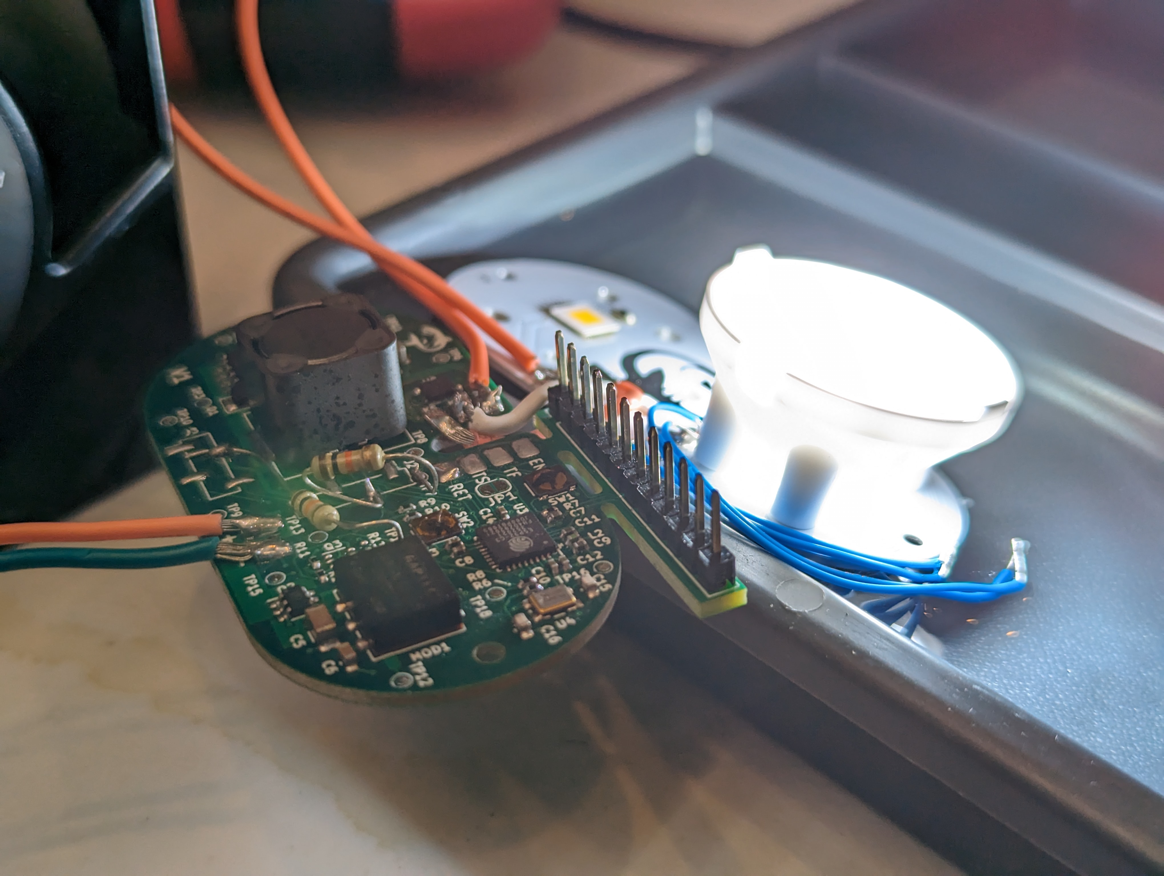
With the driver sorted, the next thing to do was to smoke test the lamps at high currents. This went reasonably well, with only one LED burning out. As you can see above, the XHP70.3 required a heat sink and passive water cooling in order to prevent burnout. Given that its running at about 42W and only ~25% of the energy is turning into light, this is a 32W heater in a 70x70mm footprint.
This is at about 70C
This is going to be very hard to keep cool, even with the die almost being in contact with the seawater. The good news is at lower settings (around 2A) I should still get a very respectable 3000 lm out of the LED- more than the sola light!
Overall efficiency from power supply to LED was acceptable- in the mid 90’s for lower currents up to about 1400mA, and in the high 80’s above that. while that might seem like poor efficiency, this takes into account relatively long lead wires to and from the pcb, the multimeter, etc, so I actually expect it to improve in the final product, especially once the thermal design is improved.
Conclusion:
This PCB needs to be re-routed with thermal concerns and strapping pins in mind, but overall, it works! This iteration has given me a lot of confidence that the final design will do what I want it to do. I’m also really excited to keep playing with the thermal camera. It gives me a lot more information than the sizzling finger test, and it lets me dig into the context and sequence of the heating.
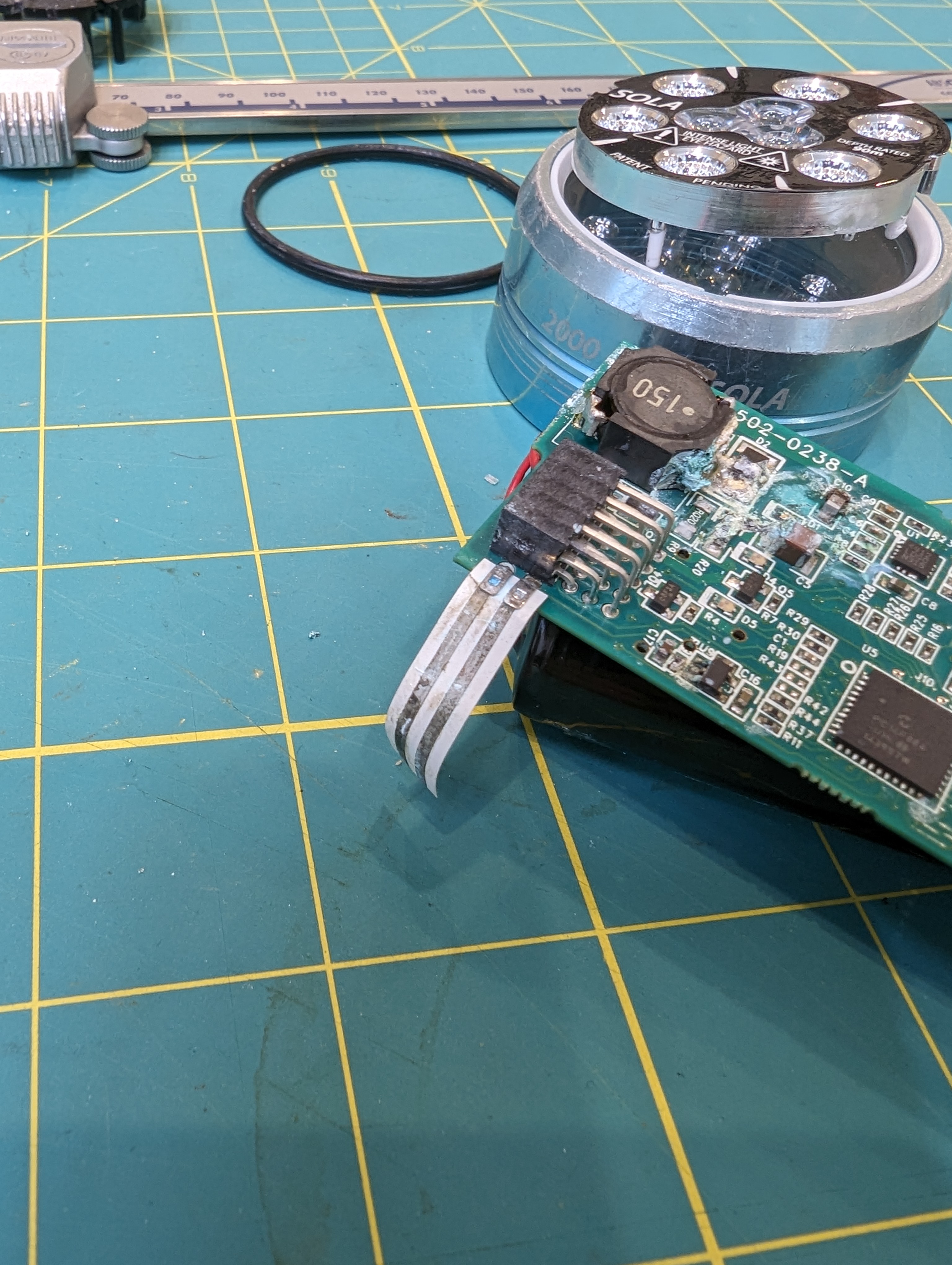
My beloved sola 2000 has finally, after many years of service (and after buying it secondhand) flooded. High power LED drivers and seawater do not mix well, and this light is at its EOL.
visible corrosion damage to the PCB
I have always wondered what was in this wonderful light, and now that its toast I don’t have any issues tearing it down to find out! There are a lot of very clever design decisions in this light, and a lot to learn.
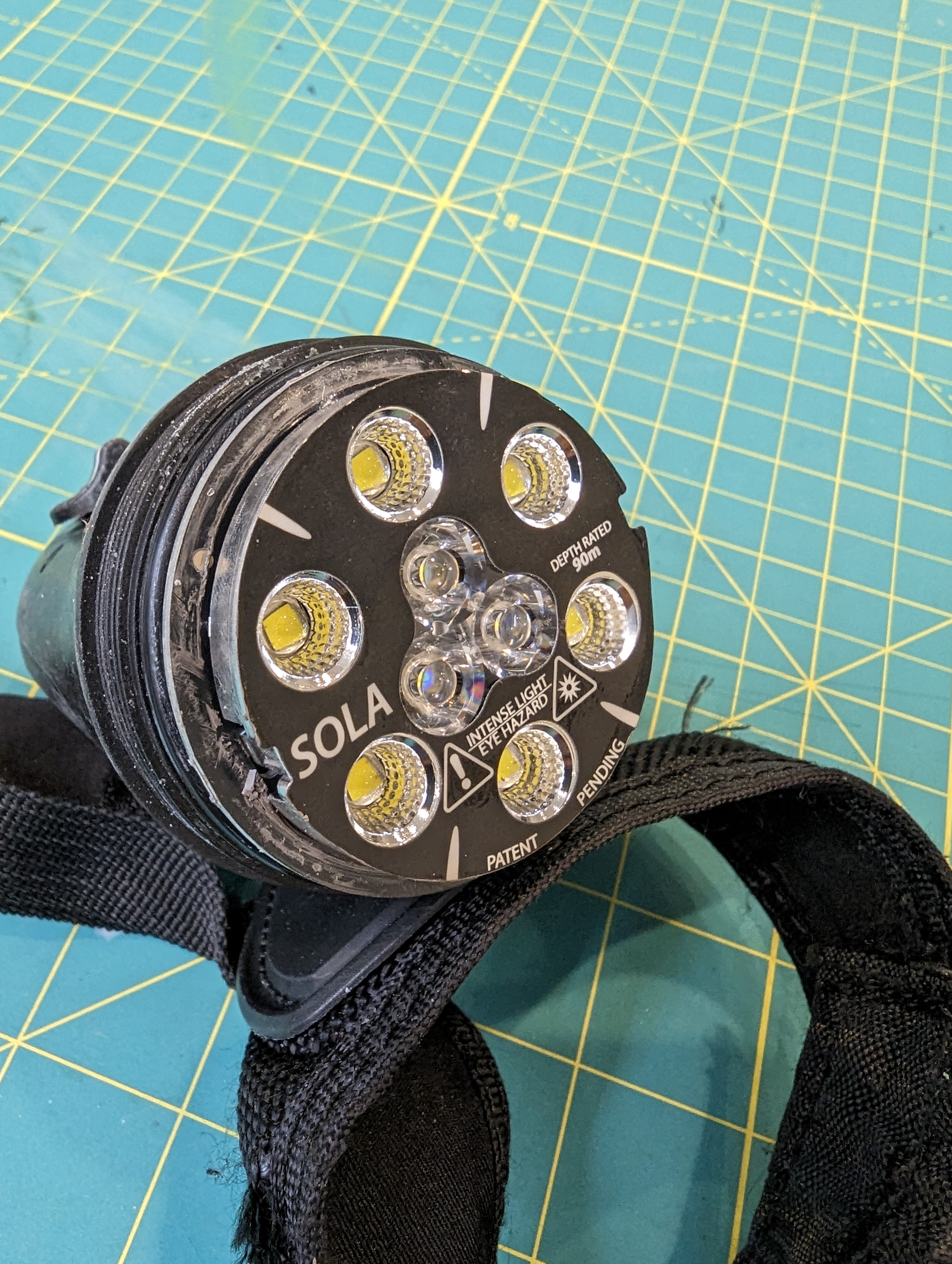
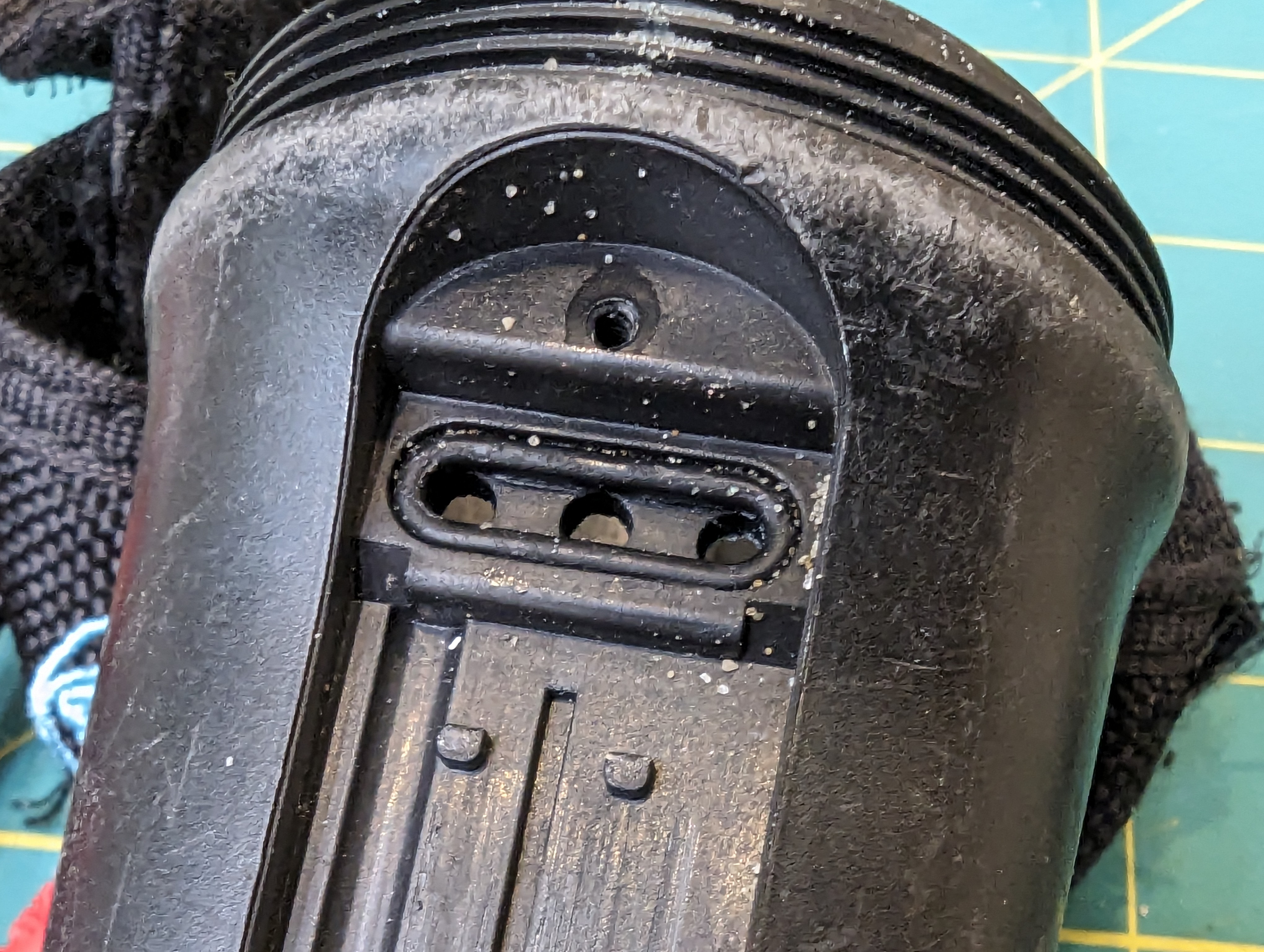
Light head
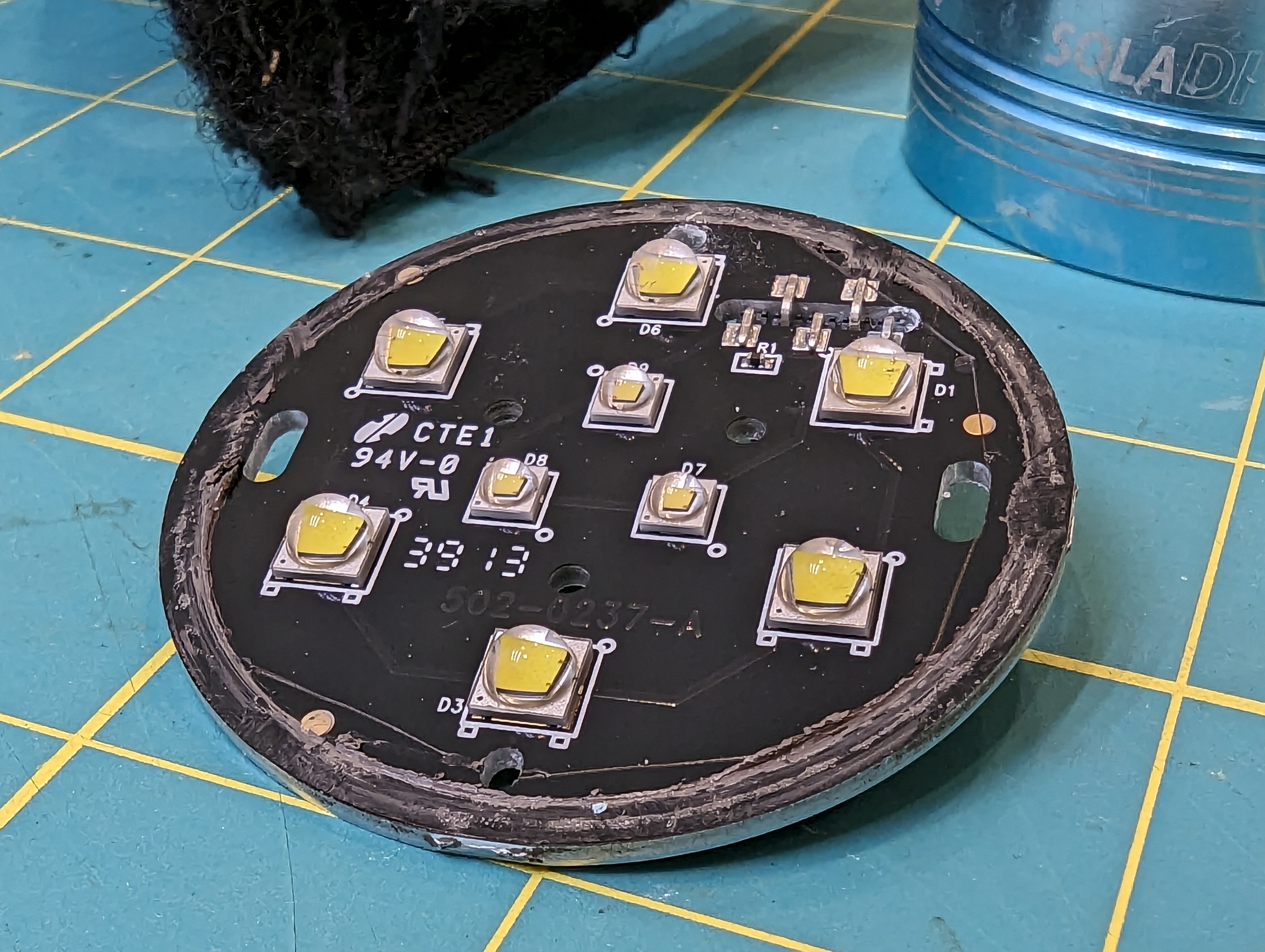
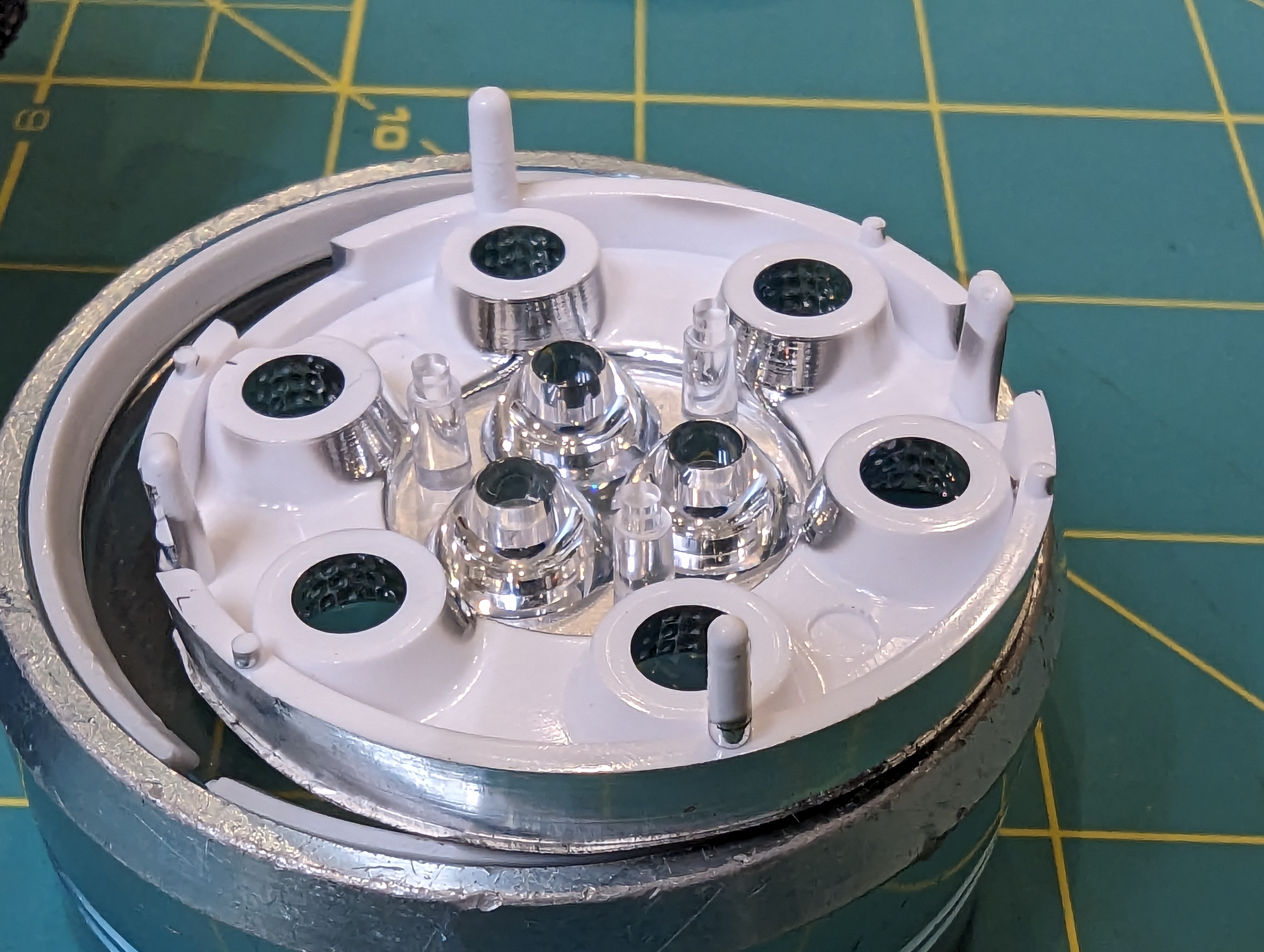
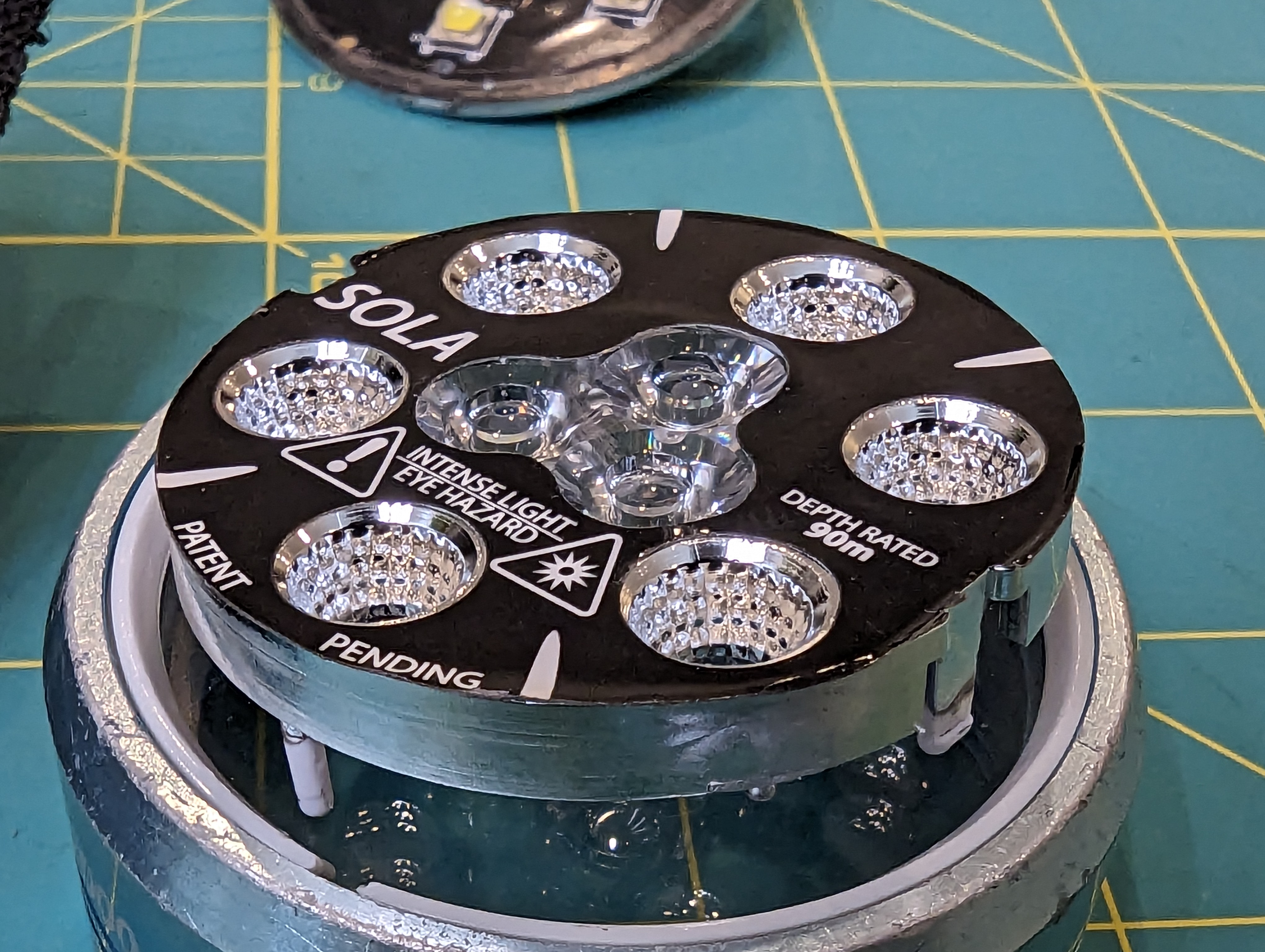
The light head has two rings of LEDS- one for spot lighting and one for flood lighting. the small inner ring of three LEDs is the spot light, and the outer LEDS are the flood light. Given the package size and general shape the LEDS, I assume the inner ones are CREE XP-E2 LEDS, and the outer ones look like CREE XM-L2 LEDs.
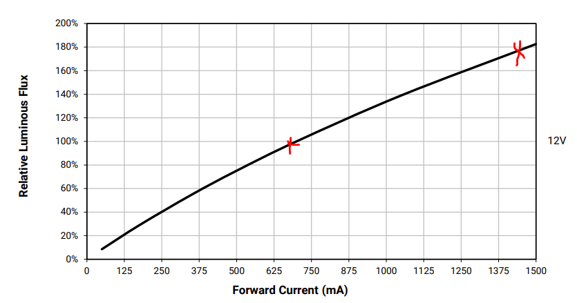
from XHP50.3 datasheet- note that 2x current does not reach 2x luminous flux. additionally, 2x current increases Vf, which makes it even less efficient than expected from this plot
Having multiple LEDs is very smart, because LEDs run more efficiently (in terms of light per heat) at lower currents. It also spreads out the heat loading of the PFB- CREE says to estimate 75% of LED power to turn into heat instead of light- that means that a 4W LED needs to dissipate 3W of heat.
Given the stated lumen output of the light, I would guess the flood lighting runs around 9-10W, or 1A at about 9V. The ring of 6 flood LEDs probably run at about the same current (1A) but at about 18V, for an output of 18W. This means that about 7-14W needs to be dissipated. This seems to be done through good contact of the aluminum PCB with the metal ring that goes on the front of the light. If you look at the PCB photo above, you will see a smear of thermal grease along the edge.
Running multiple LEDS efficiently means spreading the heat around, especially for the radial LEDs, which are closer to the heat-sinking bezel. Its also important because the light is powered by a relatively small battery pack.
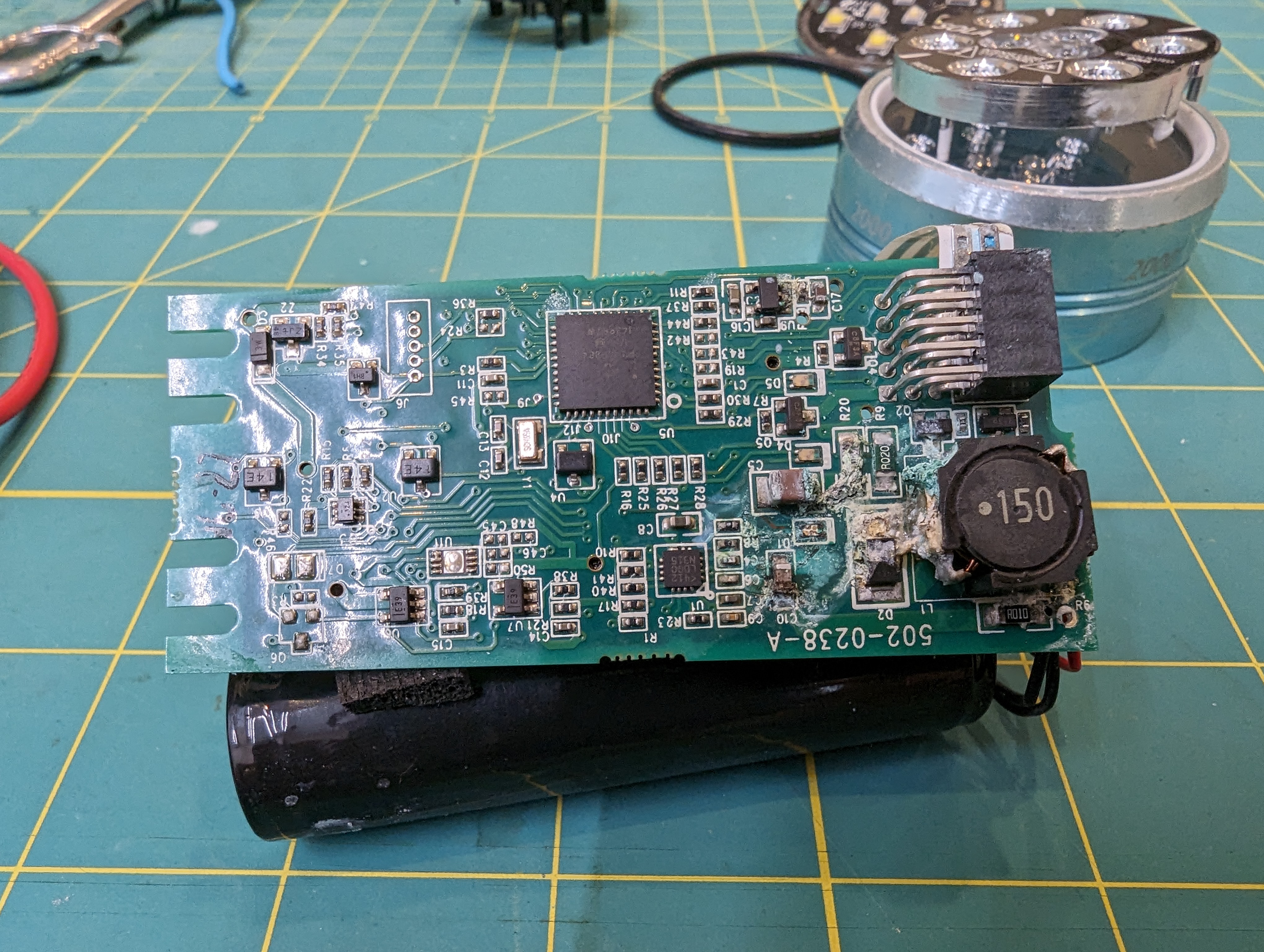
To prevent overheating, it seems like there is a single thermistor on the PCB as well. This will let the controller throttle the output when the emitters get hot.
Optics
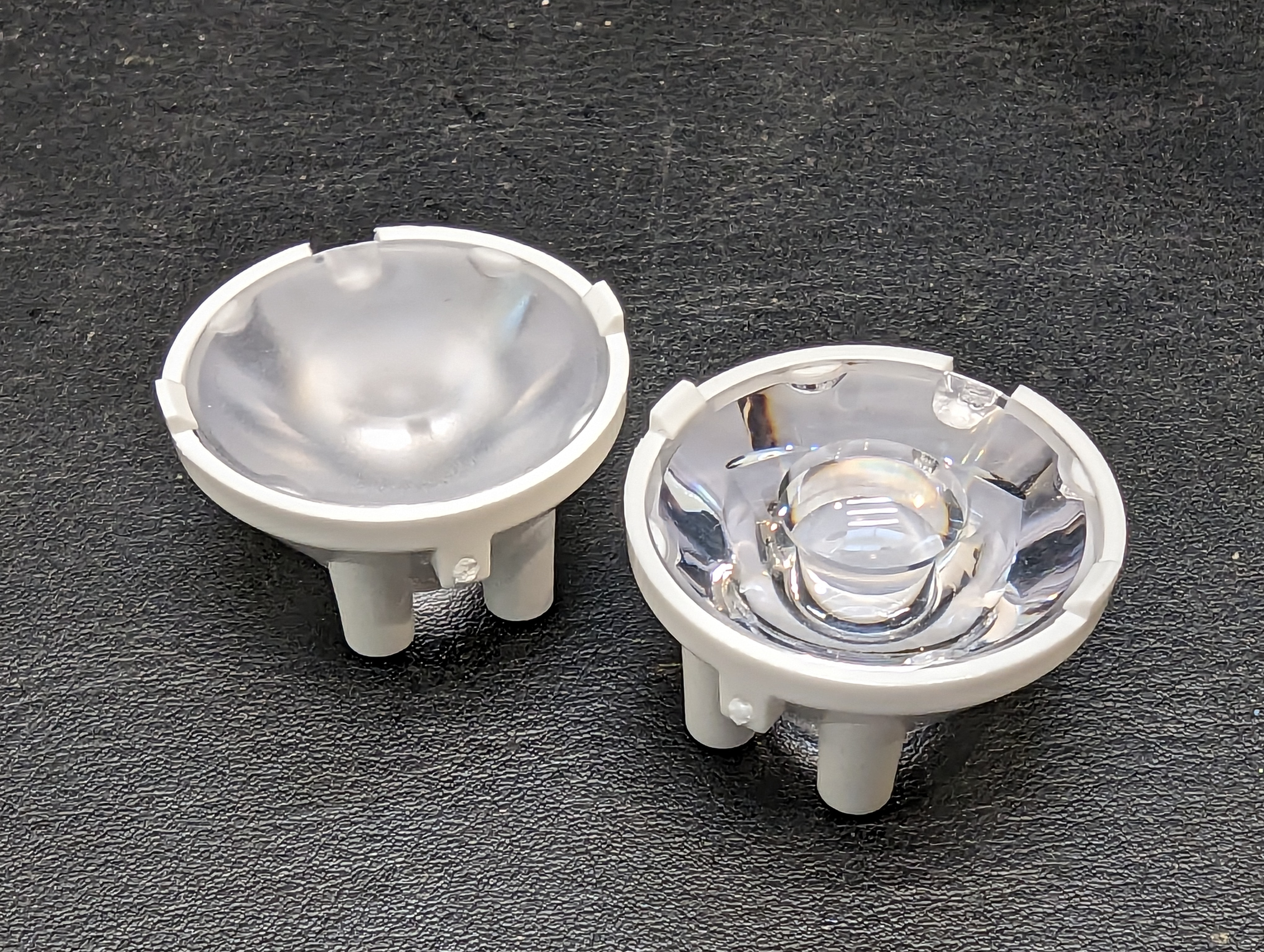
The optics look a lot like they are made by carclo (wild conjecture). There are two styles- reflectors for the spot lights, and a total-internal reflection style optic for the spot light. I do wonder if there is any attempt to collimate the spot beam to make it extra tight, by biasing the three spot beams inwards.
LED driver
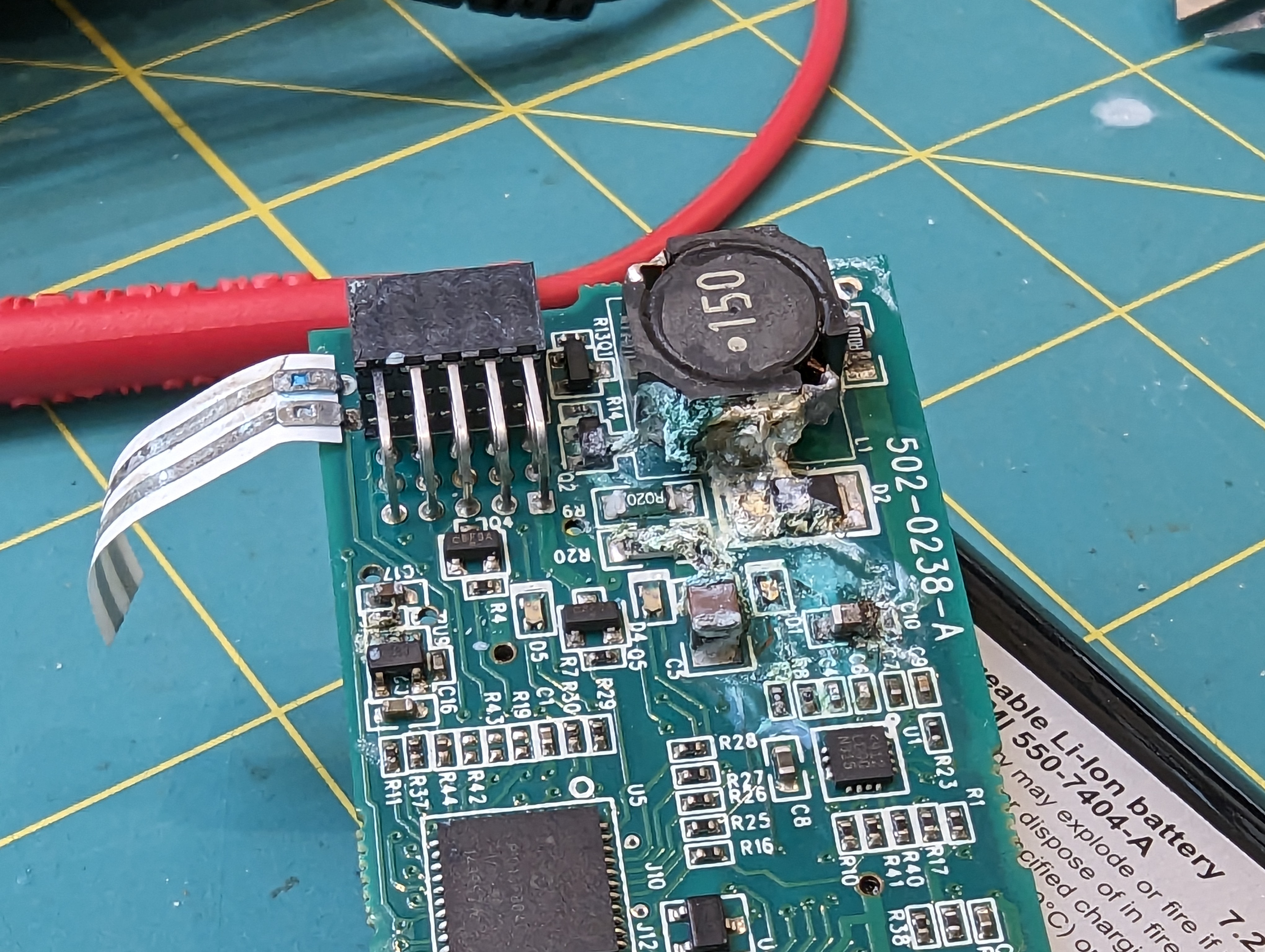
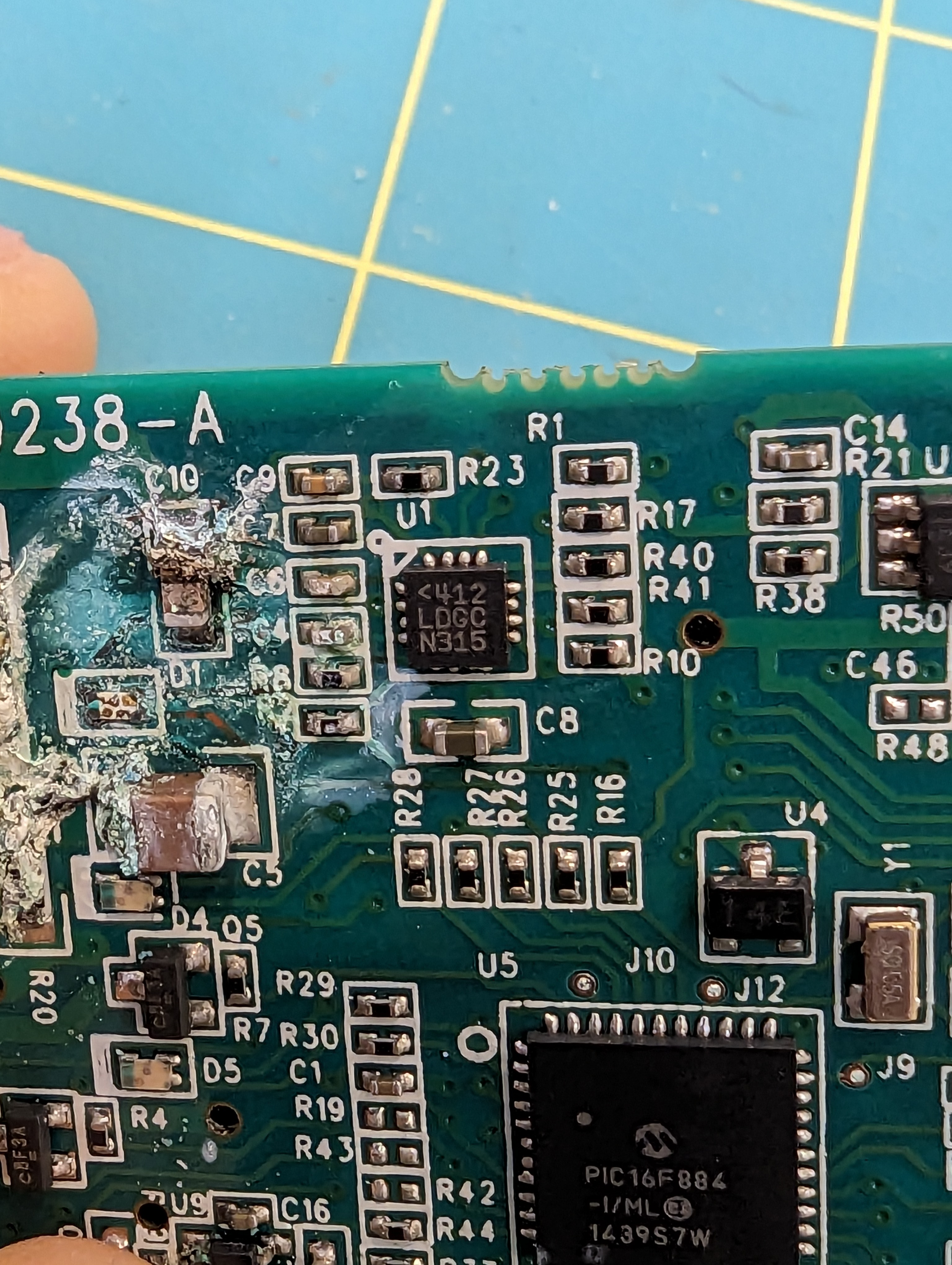
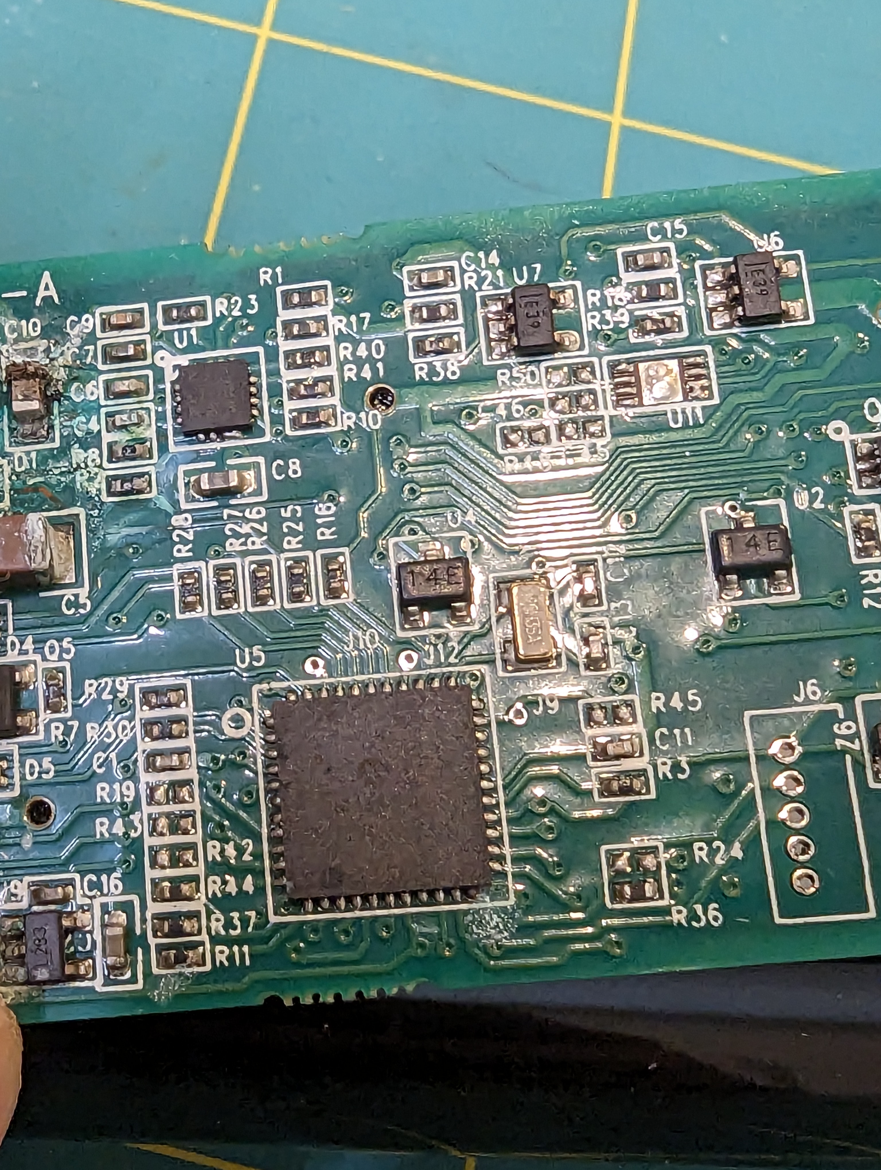
The LEDs are driven by an LT3755 wide-input rage LED driver. This driver is probably operating in boost mode all the time, since the battery voltage is too low to drive any of the LEDs. Interestingly, there is only one driver (just like in my design) but there appear to be two current sense resistors. I suspect these resistors are switched in for the spot and flood modes (on the high side, with a PFET), and then the overall brightness is controlled by PWM. This makes sense because these LEDS are probably operating at reasonable efficiency, so there is no advantage to turning down the average operating current.
As you can see, most of the corrosion/damage happened near the boost converter. It is close to where water can come in, and it is also where the highest voltages exist on the board. Seawater can cause a short between the current driver outputs, which would then tend to increase the output voltage until the current set point was reached, or until the driver maxes out or reaches some thermal limit- in other words, its a vulnerable circuit.
Flood sensor?
This board has something pretty unusual on it- a big floppy ribbon with conductors on one side. At first, I thought it might be some kind of temperature sensor, but I think it is a flood detection circuit- if it gets wet, it will alert the micro to shut down the led driver. This makes a lot of sense, both to protect the battery and the PCB. If the lamp is dried out after being protected from a flood, I imagine it would be just fine.
Magnetics + Micro
The micro is a pretty basic PIC16F884. The interface is much cooler. There are three evenly spaced IC’s marked “14E” on the PCB. I am guessing these are made (or were made) by NVE, since a lot of their ultra-low-power magnetic switches have that as a portion of the part number. This allows for control of the light without having an extra hole (leak point) in the case.
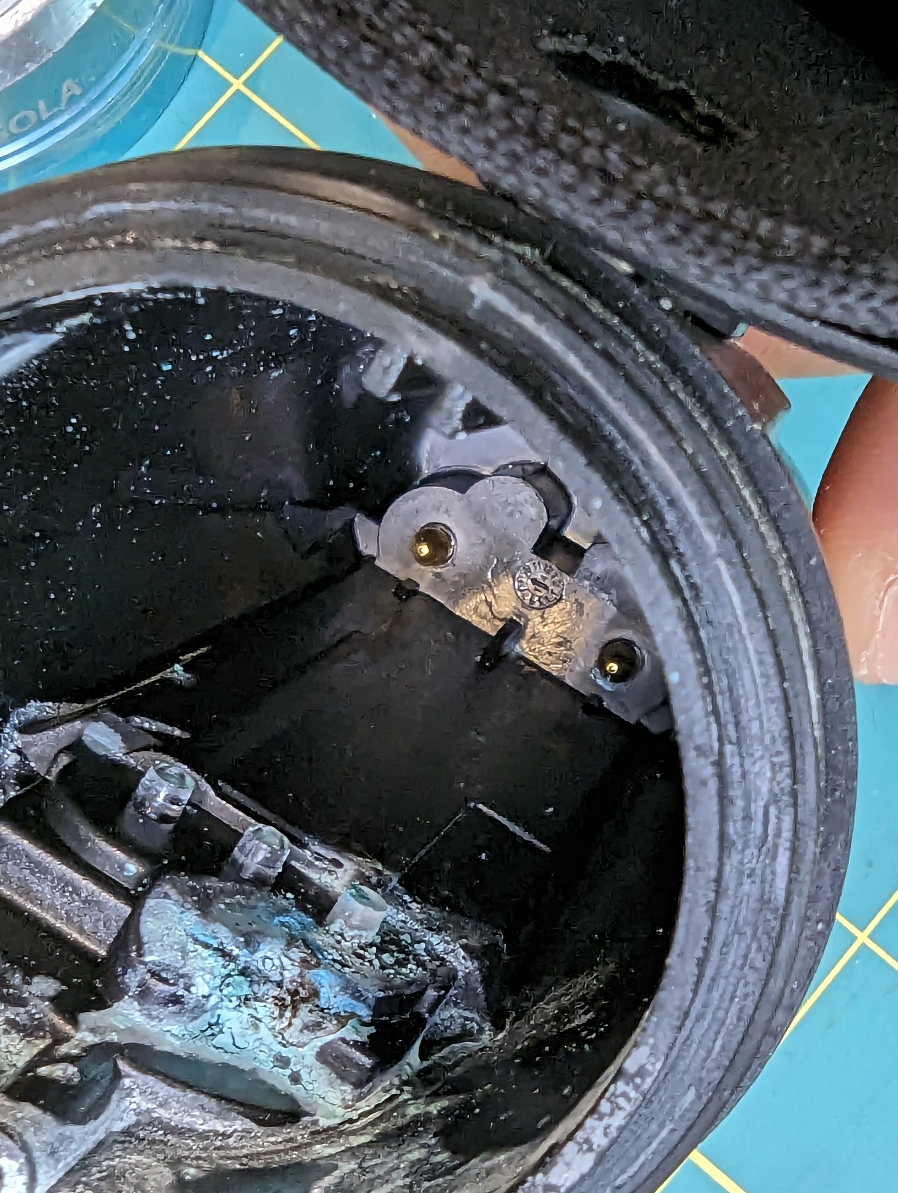
Power connections
Surprisingly, the power connections are made by wedging the pcb onto the gold contacts in the back of the case. Never in a million years would I have though that this would work so well, but some clever ribs in the back of the housing push the skinny pcb cutouts/contacts onto the gold plated pins.
Autopsy
I’ve always liked the sola lights because they are “factory sealed” and there are no waterproofing components that need changing regularly. Inspection of the front oring didn’t yield any interesting results, but looking at the light pipe seal, I have some suspicions that this might be where the light failed.
The corrosion is right under this seal, although that is also the most likely place for corrosion to happen, so its not a slam dunk. However, this is a circumferential static seal, and there are things I dont like about it.
Specifically, the surface finish of the light pipe is not very smooth on the contact area of the oring (difficult to photograph), and the whole light pipe can rock gently (although this is somewhat prevented by the bezel). The bend radius of the oring is also pretty tight compared to the diameter. The radius is about 2x the diameter, where the best practice would be about 6x the diameter.
Obviously this is a fine design, given that this light has lasted many many years. That said, I am suspicious of this seal.
Closing thoughts:
puffer-palooza at folly cove, illuminated by this light…
This light is pretty tidy from an engineering prospective, and it was a great dive light. I am still curious about what is shared between different models- how is it different than the sola 1500? from the spot lights (the driver here could easily drive a COB)? How did they reuse parts between the designs? And what on earth is that funny three-tier connector for (different models?).
I won’t be getting the answers to these questions but its fun to see what made this thing tick for so long.
I recently found out my sola 2000 torch is torched- water got in and corroded the connectors. while it might be technically salvageable, I used this as an excuse to start another project- a canister dive light. I love my sola light, but the battery does not quite last two dives, especially at full blast. This means I need to bring two lights, two chargers, and two lights, and that is a little inconvenient. It also means I spend a lot of time futzing around underwater going from low to high power mode. This is surprisingly annoying, especially since I have to use two hands to switch modes.
Armed with google, hubris, and kicad I set out to design my own dive light.
Design Goals:
The goal is to build a dive light, with spot and flood modes, just like the sola lights. I want a burn time of at least 3 hours at a reasonable brightness- this is well over two recreational dives. I want it to be a canister light so I can run it full blast for the whole dive, temperature permitting. And I want it to be about as bright as the sola lights. And small. And I want a pony to go with it (kidding).
Optics and LED choices
There are a lot of constraints on this project, starting with thermal and optical considerations. There are only so many off the shelf optics, and without much in the way of a mechanical prototyping department, I want to minimize iterations. The simplest way to do this was with single LEDs and off the shelf optics. Carclo has not only an impressive array of parts to buy, but they also have charts/images to go with the optics with different base LEDs.
The problem with single LEDS is that the efficiency of the LED suffers at high outputs. This creates a lot of heat. Hopefully I can use the ocean as a heatsink. CREE seems to make hands-down the best high output LEDS, and after some careful considerations of what is available in low quantities, I decided on one XP50.3 and one XP70.3 LED. Two XP70.3’s would be better, but the beam pattern on the spot light would be too wide, since I can only get the XP70.3 with a dome lens.
Driver
Next up was the driver. It seems pretty useless to have spot and flood lighting on at the same time, and as you can see, the PCB does not have a lot of room on it for another big driver and inductor. Instead, I intend to share the high-side LED driver across both LEDs by low-side switching them. The header on top is for programming, and as a breakout for interesting pins.
Microcontroller Selection
I begrudgingly picked the ESP32 as my microcontroller. It seems like a shame to have and not use a ton of the peripherals on there, but its cheap (compared to an attiny), small (but still has a lot of pins), and in stock (unlike the atsamd series). This requires a 3v3 regulator, and due to size and laziness constraints I opted for an integrated DC-DC module. These are awesome, cheap, and easy to assemble, which is nice because I already had a lot of 0402 parts.
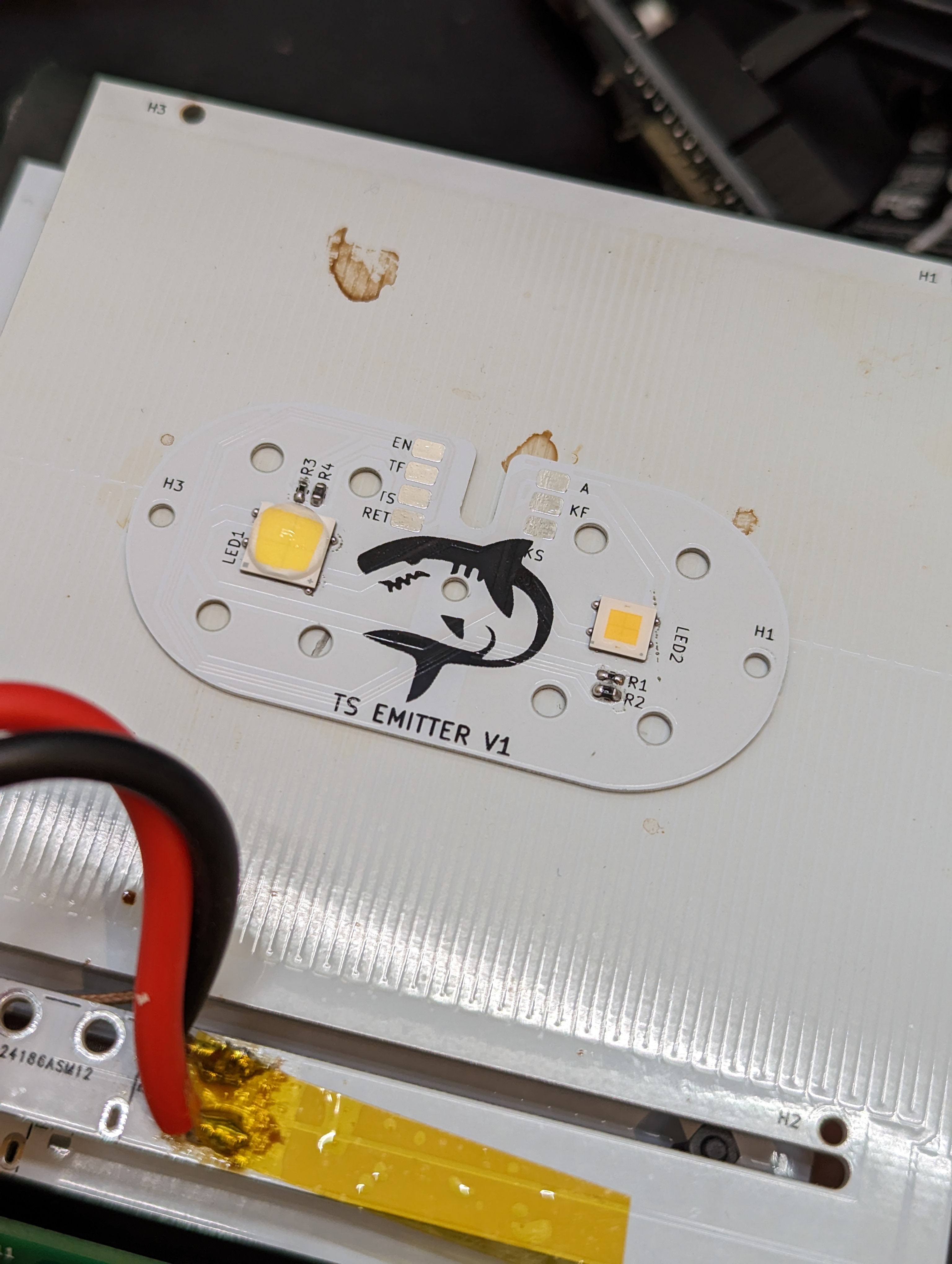
Emitter (LED) Board
The emitter board is aluminum, for better heat conductivity. At full blast, this will need to dissipate ~30W! In addition to LEDS, there are a couple thermistors for temperature measurements, placed near the LEDs. Given that each LED is a multi-watt heater that could probably melt itself off the board (with low temp solder), it seems prudent to monitor temperatures.
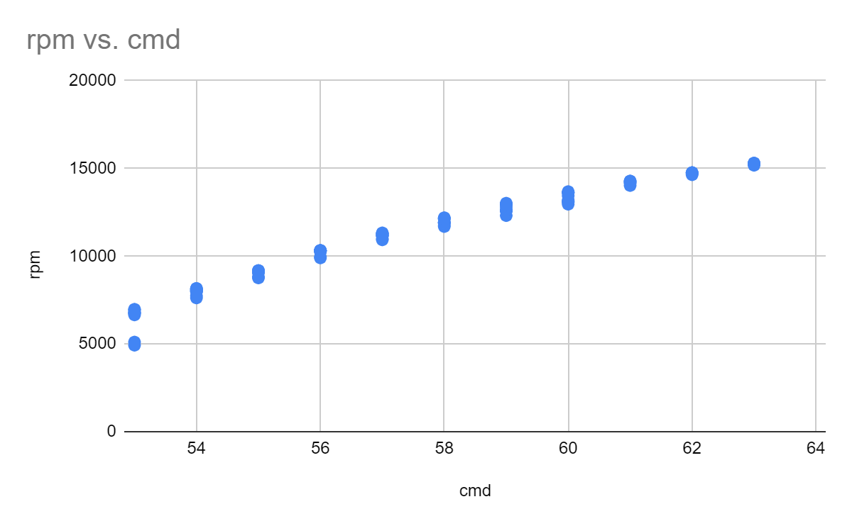
With the tachometer done, the next step was to get the ancient BLDC and ESC wired up and figure out how fast they were spinning. I know that the motor spins very fast but I really didn’t know how fast it was. It turns out that the speed is mostly too fast.
Here I plotted the RPM vs input command, which is basically in “hobby servo degrees” since that is how the ESC expects to get commands- a pulse every 20ms where the width of the pulse corresponds to…something. I mostly care about speeds between 5-10k, which gives me about 4 settings. I suspect that by decreasing the voltage of the power supply, I could decrease the minimum speed by limiting the free-run voltage across the motor.
As I said, its not clear exactly what the mapping is from pulses to rpm, since I don’t really know how the controller works- is it closed loop? is speed control achieved with voltage limiting, or is there actually feedback? Right now it doesn’t matter since my goal is just to make things spin fast. As you can see here, the motor spun fast enough that the tape I was using as part of the encoder ripped itself off and disintegrated all over the inside of the container.
Next Up: A PCB
absolute chaos
Based on a lot of really annoying fiddling and having parts get de-soldered during assembly, I have decided I really need a PCB for this project to prevent it from self-destructing by vibrating my deadbug soldering apart. A display, and maybe some buttons would help make it fully usable.
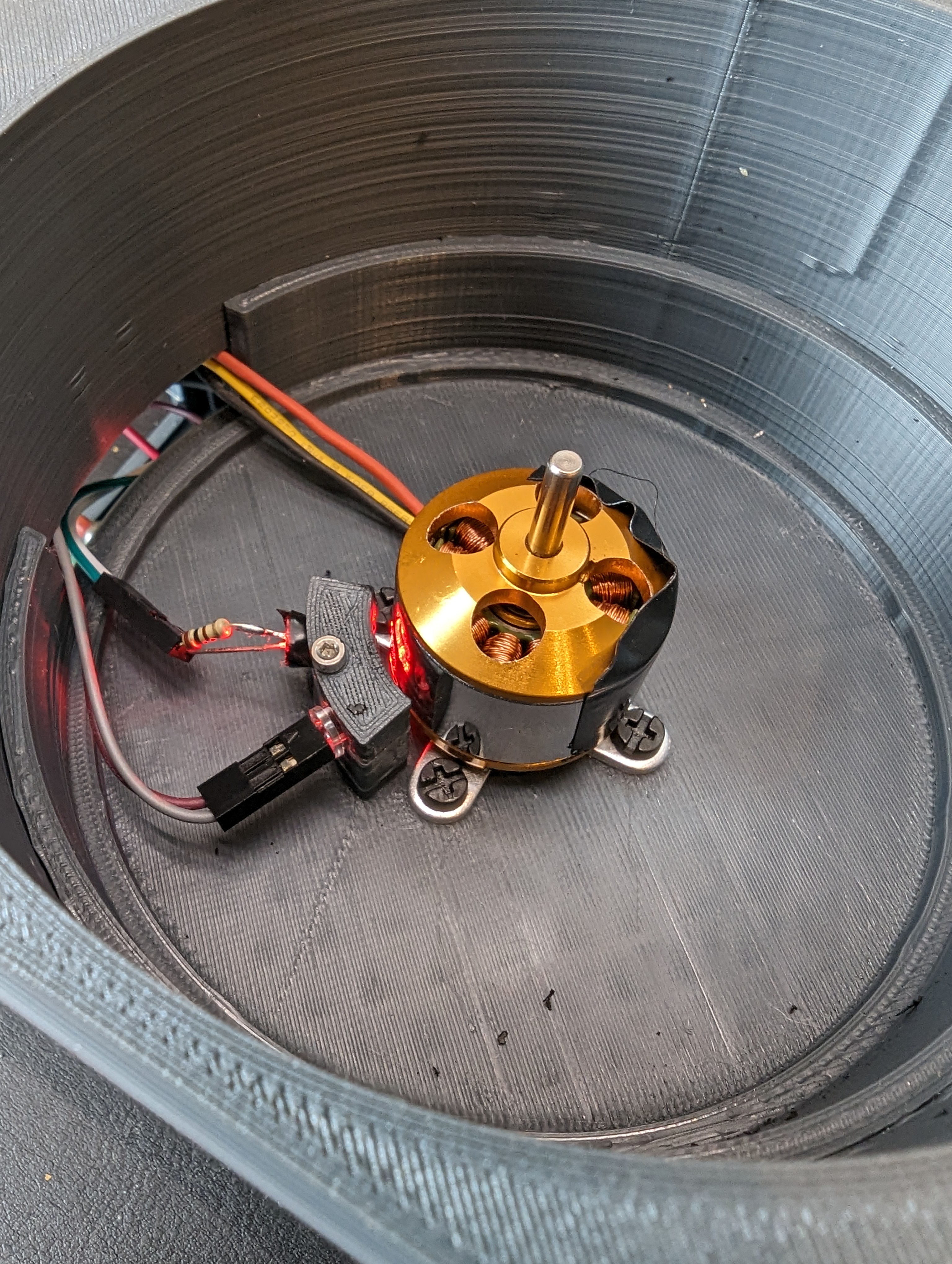
I ended up with a day to work on my spin coater in between a few other projects. Originally, I wanted to make a nice spin coater but because I am basing the design on a random ESC and motor that I bought 5 years ago, I decided the rest of the build would come from the junk bin as well- at least that would be fast.
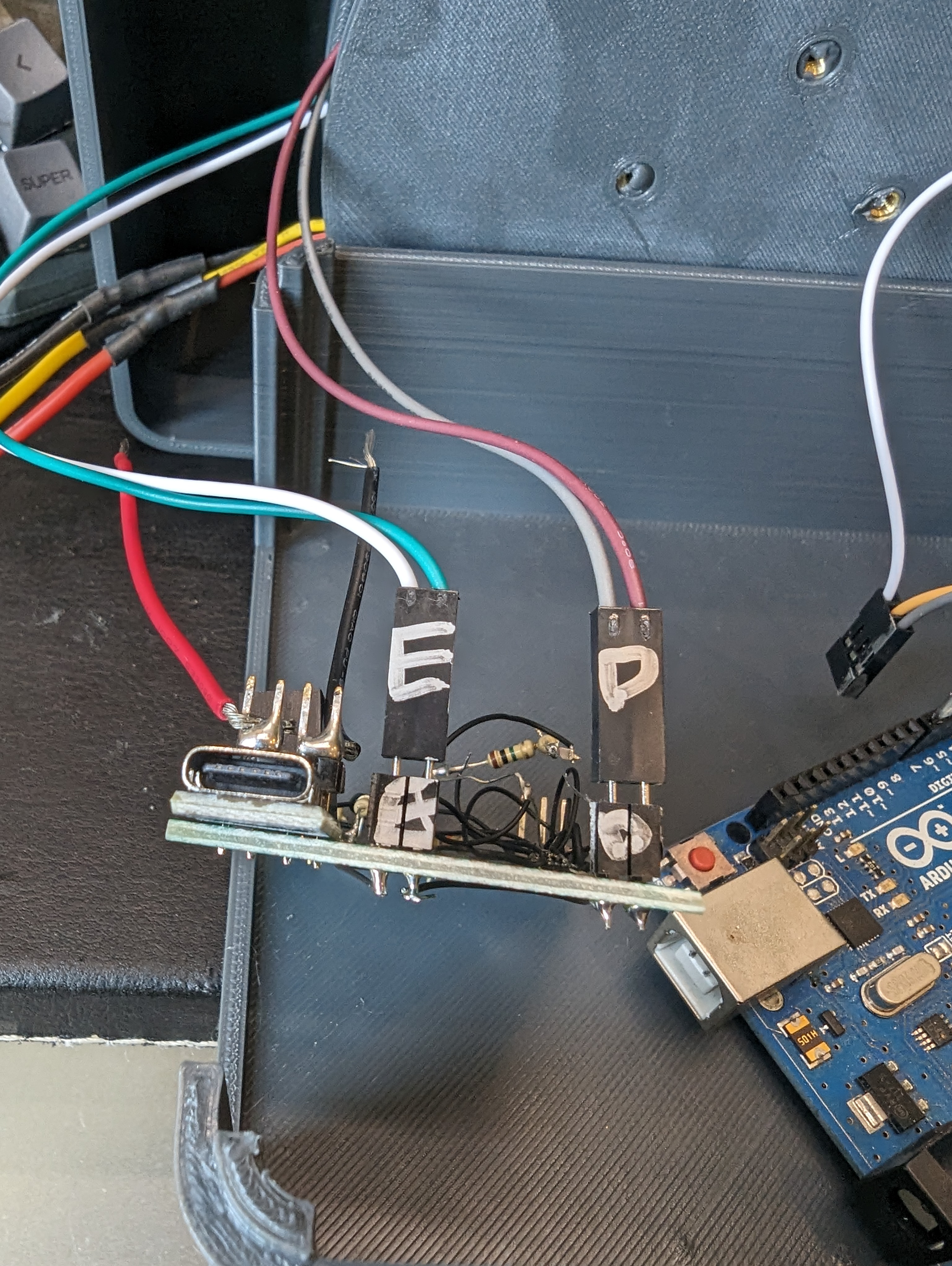
One component I don’t often use (aka have in the junk bins) are “fast” analog light sensors, like the kind you would use for a tachometer. However, I do have a lot of LEDs, and I managed to find one single op amp part in my junk bin, and so I figured I could either spend a day designing a pcb that would come in 2 weeks, or spend one day hacking together a tach.
My goal was to get a digital signal out of the system, where one rising or falling edge corresponds to one revolution of the motor. I want to run this motor from about 5-10k RPM, which means each revolution is 100 uS. Detecting something every 100uS is pretty slow in circuit land, so I was not worried about the speed of the electronics.
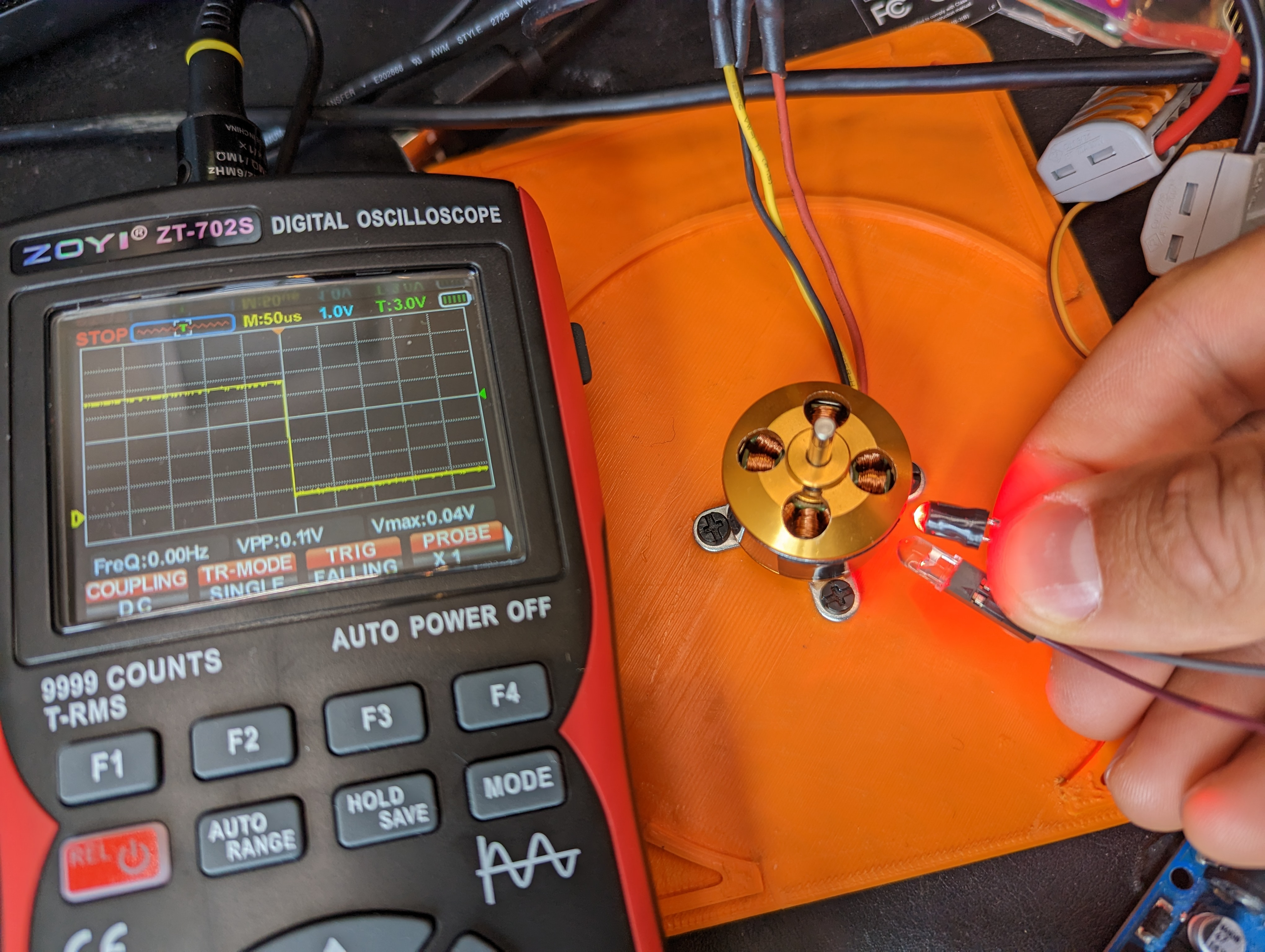
LED as a photodiode
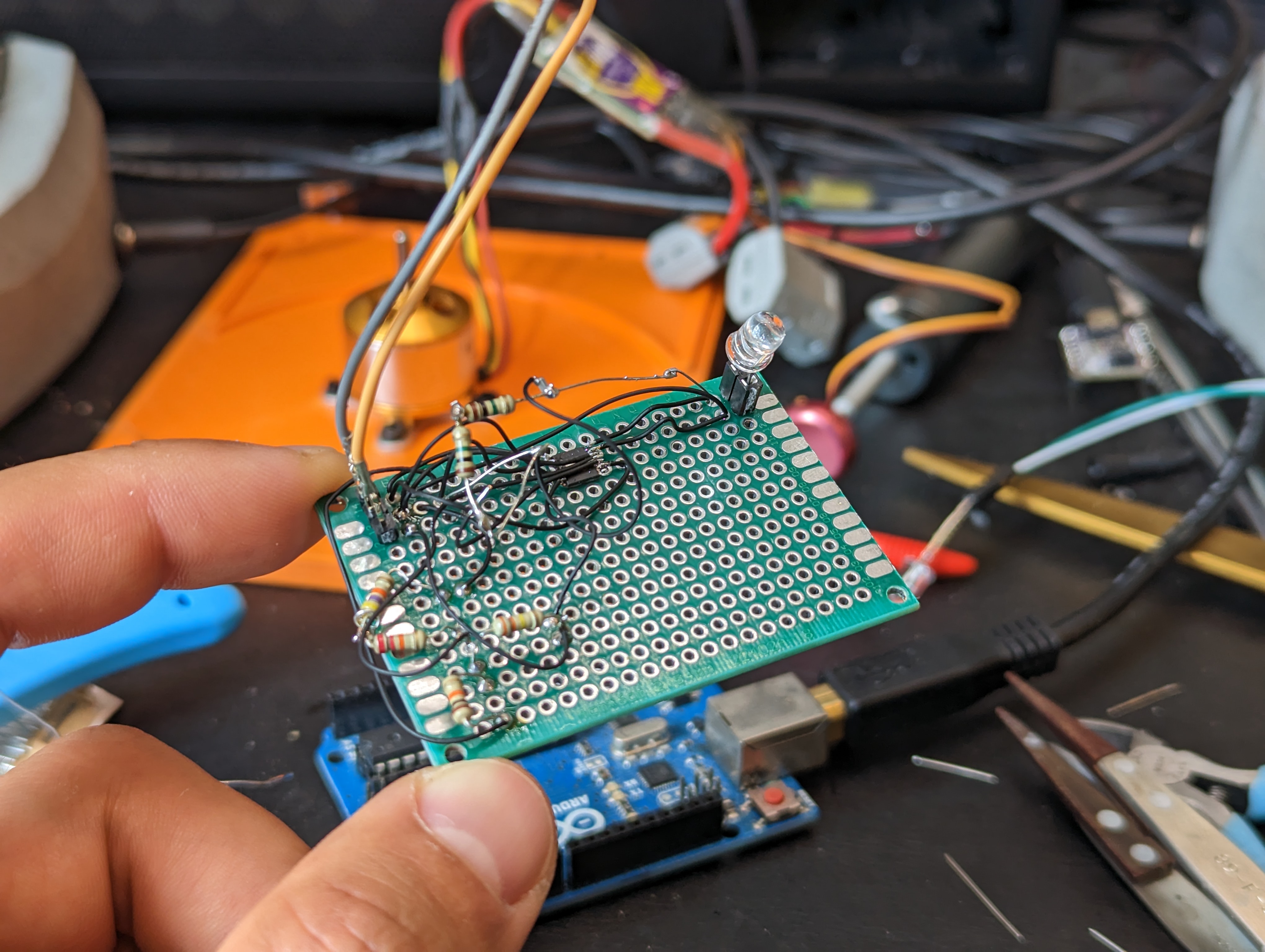
I know that an LED can be used as a tiny tiny current source, and that there are two common ways to amplify it- with a transistor or with an opamp. I tried a transistor to start, since I knew I had some 3904s stashed away from an old project. However, this did not give me enough gain- the signal was only about 100-200mV with a bright light shining into the LED. I didn’t try the darlington pair, because later I found out I did have three (3) dual op amps in my junk bin.
I ordered three ALM2403QPWPQ1’s for some reason in 2021. I have no idea why, but I was pleased to find out that I had an op amp on hand. Fortunately, these are .65 mm pitch parts- that makes a big difference compared to .5 mm pitch parts for unaided hand soldering, deadbug style (note to self: buy microscope).
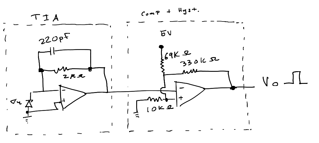
With these dual op amps, I could actually get everything I needed out of a single chip. The first stage is a transimpedance amplifier with the photodiode as a current source. This takes the current generated by the photodiode and turns it into a voltage. In theory it should be pretty linear with incident light, but I didn’t test this.
Since I have no idea where my LEDs came from (junk bin leds!) I just stuck in the values from the make article linked above (by Forrest Mims). This seemed to work well enough, but and testing showed that increasing the feedback resistor to 2Mohms gave me suitable gain, with an output around 1.5-2V. This signal gets fed into a comparator block later, so the actual value is not too critical- just that the signal has a wide enough swing.
The comparator block is built out of the second op amp, resistors I had lying around, careful soldering, and this app note on adding hysteresis a comparator. I had to tweak the values to the resistors values I could make, but after some simulation I got a suitable result. Here you can see the .2 V of hysteresis in a plot of input vs output voltage.
As you can see in the title photo, this produces a nice clean edge as the motor body (shiny) transitions to the tape (black, not shiny) that I stuck on it. Now its back to the mechanical drawing board to make a platformt to test/write software, and time to order a VERY simple PCB for when my questionable soldering starts to fall apart.
New Tool: ZOYI ZT-702S
A one new tool that made this way easier was the ZOYI ZT-702S. I bought this to augment my basic multimeter. I was skeptical of the oscilliscope feature after suffering through quite a few substandard scopes.
It turns out to be a total delight to use, and it is great for simple stuff like this where I want to look at some quickly changing value or to measure a rise time or to see if a signal is ok. It physically much easier than breaking out my big scope (because the big scope is VERY big). The portability also seems awesome- I have done all kinds of nonsense where I need to measure a sensor in the field and a multimeter is okay, but a very basic scope would be way better. This thing rules! It can even take screenshots, and the menus are straightforward.
My main gripe so far is that the auto range button exists- since its next to the hold button, I press it by accident sometimes and this resets my measurements and puts the scope in AC mode, instead of restarting the triggered data.
As a basic multimeter it also does fine, and the continuity beeper is very fast, and the probes are pretty nice. I am excited to add this to the toolbox!
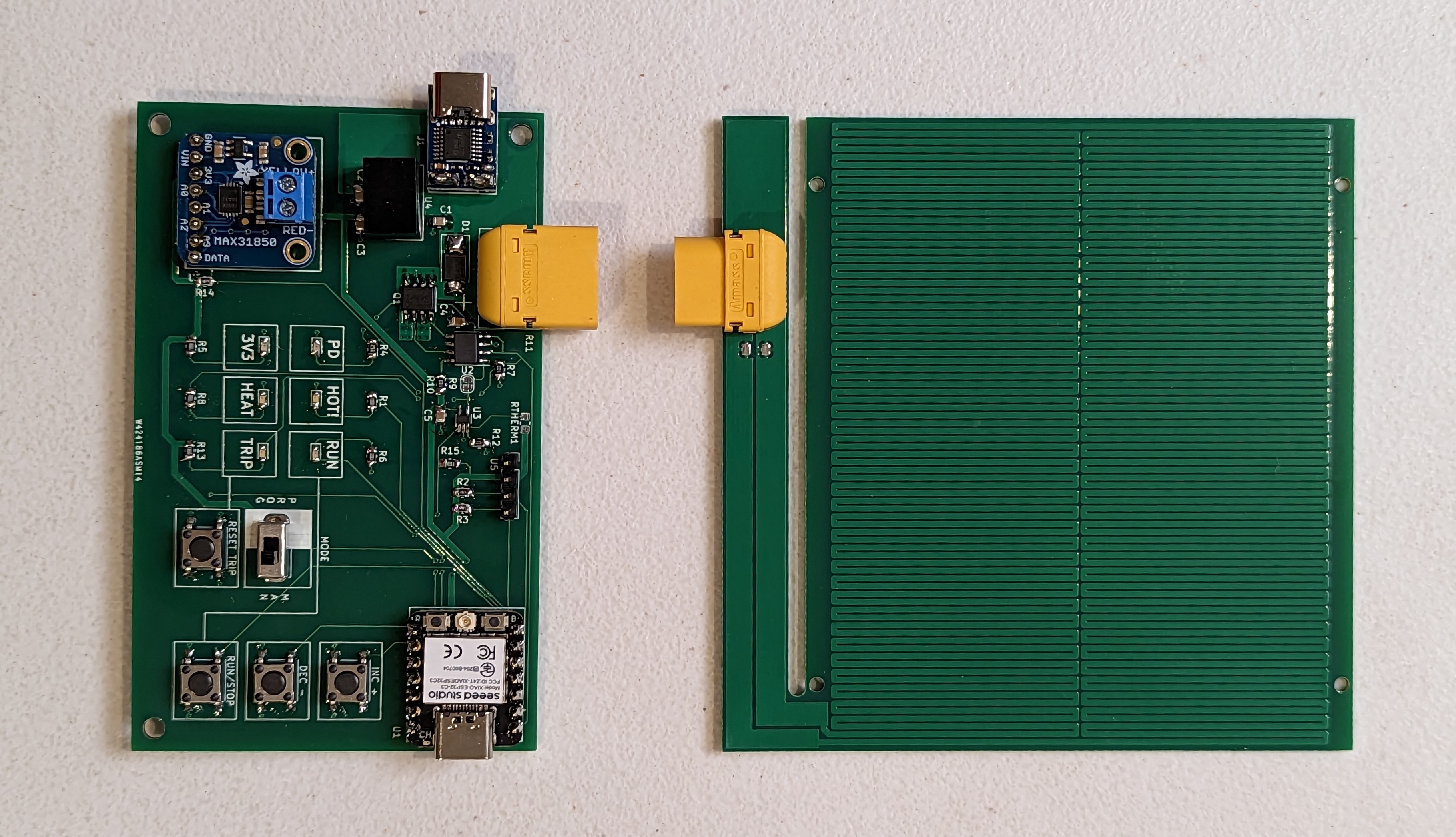
The hot plating continues! And with the boards actually in hand, I can compare my estimates to some real world measurements.
In the end, I made both FR4 and aluminum heaters. These heaters ended up having slightly different properties. Oddly, the aluminum PCB has a higher resistance (4 ohms) than the copper pcb, 2.9 ohms). Read on to figure out what this did to the design.
Designed Vs Measured Resistance:
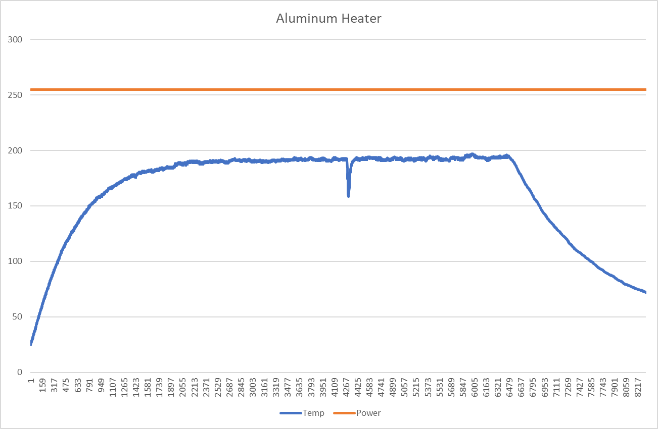
The design resistance of the heater track was 3.3 ohms. Clearly, this was not “nailed” for either of the boards, but it was close. I was surprised that both boards didn’t overshoot the resistance, due to the addition of a few extra squares of conductor on the connector island- however the FR4 heater seems to have a more generous allotment of copper, and the aluminum PCB may have slightly less copper.
Unfortunately, this means that at higher temperatures, the power delivered to the aluminum board is much lower than desired. The calculated value for the resistance at 200C is about 6.7 ohms, and the measured value is 7-8 ohms. This means that the maximum power available at 20V is 50-60W, or less. This is pretty close to the theoretical minimum power needed to reach 200C, which is why this plate struggles to achieve 200C. As you can see, the heater is on for the entire time (until I pulled the plug). Time units are in 10ms intervals. Fortunately, this validates the power delivery assumptions I made in the past post.
To recap, Qdot is the amount of heating power needed to sustain a particular delta T, given some convection parameters. I assumed a delta T of 175k, with an area of about .01m2, and h being 25 W/m2k, resulting in a power delivery at the heater of 43W. while this is not totally spot on, its in the right ballpark. It suggests that lowering the resistance and actually delivering 100w would be very helpful to removing this 200c limit. I think 10-20 is a reasonable conservative estimate of convective cooling, but its conservative in the wrong direction if you are designing a heater.
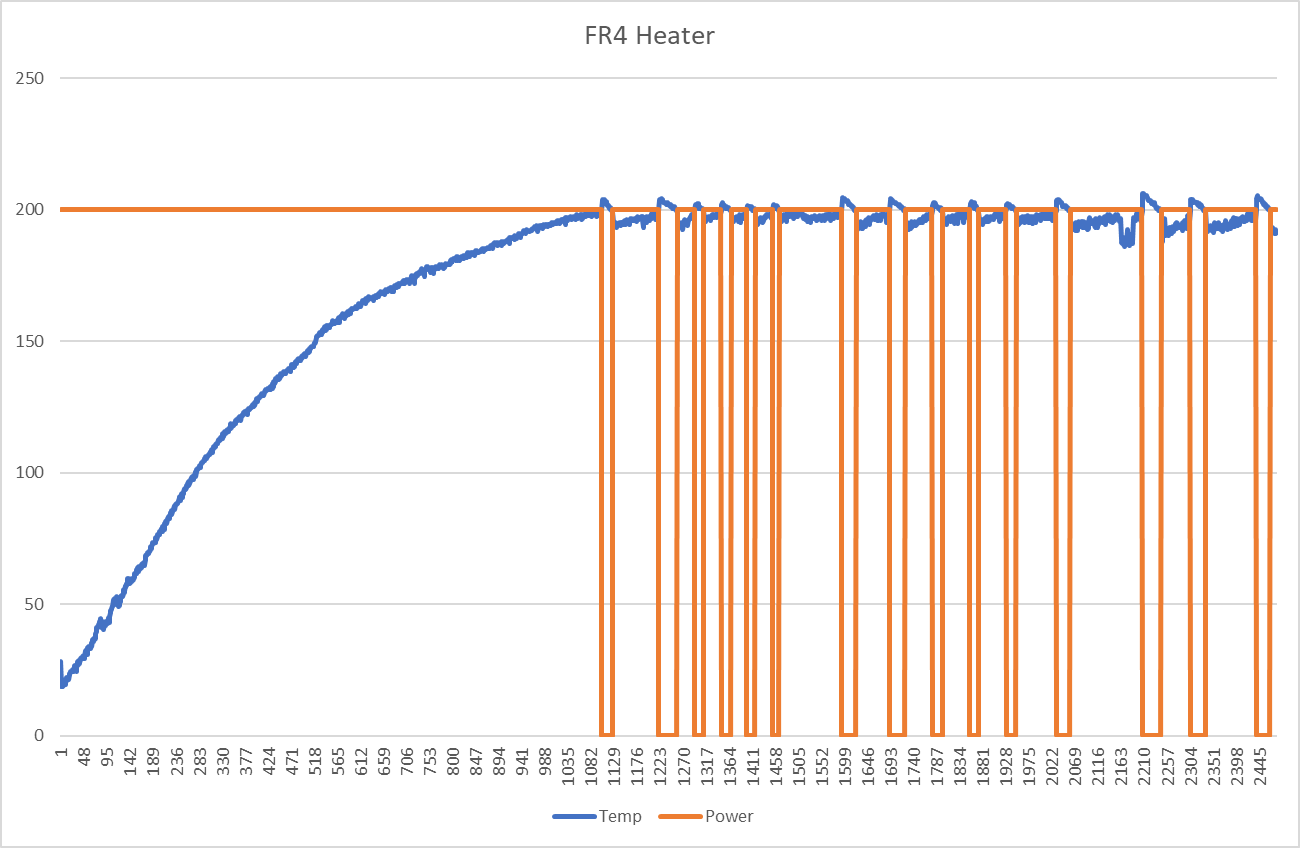
On the other hand, the resistance of the FR4 heater is low. At low temperatures, running at 100% PWM (all on), will cause the power supply to brown out. This means that the power delivery actually needs to be cut back (PWM’ed) when the heater is cooler, so that the overall current draw is lower. Once the heater is in the vicinity of 100C, it can be run “full blast”, aka more or less shorted across the power supply.
Does It Blend?
Both the aluminum and FR4 heaters were able to reach 200c depending on the conditions. Both were capable of melting solder directly on the plate, as you can see. The aluminum heater would benefit from an improved (lower resistance) heater trace.
The remote probe feature allows for the sensing of the temperature of the PCB being soldered. This is good, since that is where the temperature actually matters. This can cause the heater to get much hotter (20c or so) than the top of the target board, which in this photo, resulted in some discoloration of the solder mask of the heater.
Temperature Gradients and Overheating:
The hot plate design needs to achieve two tasks: be cold at the connector (so as not to de-solder it), and it needs to be hot (and ideally, evenly hot) across the surface.
The worst case for de-soldering the connector is with the aluminum heater, since the aluminum substrate should conduct heat pretty well. Up at peak temperatures, the connector area only got to about 85C. Certainly warm, but not nearly hot enough to damage the connector.
In terms of heater gradients, the aluminum PCB had about a 10C difference from the center to the corner at 200c. The gradient to the “neck” of the connector island was much worse (13+ C), since the thick traces there (and the substrate) act like a heat sink. The corners are cooler since there is some radiation and extra convection out of the sides of the heater.
The FR4 board has a even higher gradient, in excess of 50C during heat up, and staying steady at about 50C after several minutes. This is annoying, since it makes the outer areas of the PCB too cold to solder on. The center can be overdriven to compensate, but that leads to overheating and discoloring the solder mask.
New Design Goals + Limitations:
Its clear that hot plate soldering is not the ideal way to solder- something like a toaster seems a lot better and faster, since it can more evenly heat the target PCB. The main issue is that in order to get the top of the PCB hot enough to reflow, the bottom has to be quite a bit hotter. This is worse with traditional lead-free solders, since they need to hit about 220C. Lead-Tin eutectic solders need to hit 185 or so, and bismuth lead-free solders only need to reach 140 C (there is a medium caveat here).
You can see the results of this heating on an adafruit board (above), that I gently reflowed. The left board is new from adafruit, and the right one is reflowed. It didn’t really damage the board, but it certainly would be an unacceptable outcome if a manufacturer overheated a board like this, and the lead free solder (I assume) on top barely reached the liquidus point, and would re-solidify as soon as I moved a component.
The medium sized caveat is that any lead in the process can poison your bismuth solders forming a bismuth-lead crystal that has a very low melting point (95C!). I think the jury is still out on using bismuth solder for stuff that gets hot, but for most prototyping it seems fine. For low temperature solders, the hotplate is fine because your whole board stays under typical soldering temperatures.
For leaded solders the hot plate will likely also work ok, since the heater can be at about 200c and the surface of the target PCB can be at 180. However, for lead-free SAC (Sn Ag Cu) alloys, I think the hot plate will likely damage the solder mask of the target PCB. However, using the PCB hotplate as a preheater could work fine, with the addition of a hot air gun assist.
I would like to use this hot plate to solder and test complete prototype designs, with packages that are hard to hand solder, particularly leadless stuff like QFNs. I find solder fumes to be irritating (and there are more at higher temperatures), and so I am going to try using the bismuth solder, at least for prototyping. For leaded work, I’m pretty sure the hot plate would work fine, and it will be a good tool (combined with hot air) for reworking SAC alloy lead-free boards. I’d also like to take up less closet space than a toaster oven, so I think the project does have some value. It also fits in nicely with the USB-C powered soldering iron ecosystem.
Electrical Stuff:
In the previous posts I shared some choices around the electrical system. The two concerns I had were not shorting out the power supply, and preventing inductive spikes from exceeding Vdsmax.
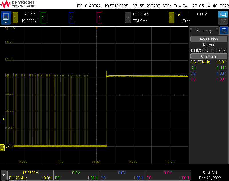
The Vgs, shown above, was totally fine since it was limited by the free-wheeling diode. Even with a 1ms charge time, the inductor failed to exceed 25V and there was very little ringing. The Vdsmax is about 30V, so there is plenty of margin.
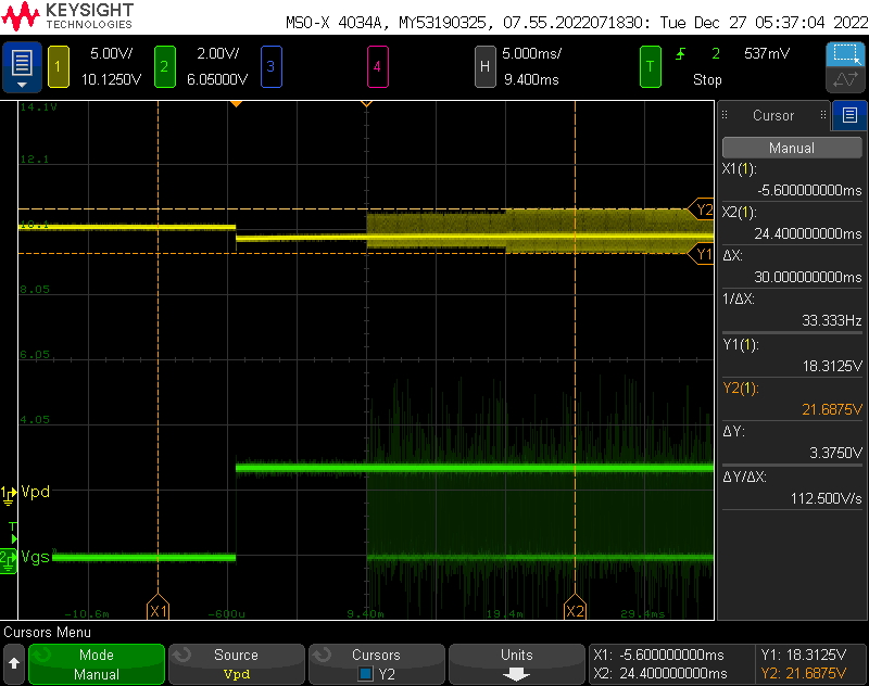
To test power integrity, I wrote some code to turn the heater on different power levels for 10ms, starting at 100% power. As you can see, 100% power reduces the output voltage just a bit, to 19.5V. This is well within the PD specification. When the PWM begins, the power supply seems to tolerate some relatively large spikes/dips as the heater (inductive load) is switched at 25kHz.
Electrical + Control Improvements:
To get a truly performant hotplate, the resistance at 200C needs to be less than 4 ohms, so the full 100W (or close to it) can be used to maintain the target operating temperature. Doing this is tricky, because it means that at 25C the heater can’t be operated at 100% duty cycle. Basically, power is not a function of duty cycle, but of duty cycle, temperature, and board characteristics.
There are two approaches to solving this problem. One is a per-heater lookup table, that lists a reasonable safe duty cycle per temperature. This is limiting since it would need to be generated per-heater, but its not unreasonable to do that given that I will likely stick with a single heater, and most heaters should be pretty similar.
Another approach would be to add a current monitoring to the USB PD supply, and cut the heater power off once you get close to the limit. This requires a relatively high bulk capacitance to provide current, even at 25kHz, but its certainly achievable. Overall power could be modulated by adding a dead time in between heating cycles, in order to follow a temperature profile. Higher frequencies could be considered, taking into account the switching time of the low side FETs. This is basically a current-controlled buck converter.
I’ll likely stick to the first approach for now, since doing current limited control requires more hardware, and it is unlikely to really improve the outcome of my soldering.
Mistakes + Takeaways
There were a few minor circuit goofs, and some things that went surprisingly well. Here is a small list, that might help you or me in the future:
GPIO9 and GPIO8 on the ESP32 C3 are bootstrapping pins– they control what the ESP does when it boots. I connected one of them to a switch, as an input for the program. This meant that the ESP would not boot into my program, but it would boot back into bootloader mode (and accept new programs). Toggling the switch made the ESP behave normally. Note to self: use these pins carefully.
The pinecil is a pretty beefy iron. It had trouble soldering to the aluminum PCB, but with boost mode and patience it had enough power to solder directly to a 3mm wide trace on an aluminum substrate. It had NO trouble soldering XT60 connectors to large pours. Don’t let the small size fool you- it is a real iron.
It is a good idea to put indicator LEDs on things like the actual power rail and the actual HEAT signal. It makes it unambiguous that something is really happening, and that the heater is getting hot.
I added a solder jumper to the overtemperature cutoff circuit. I accidentally swapped the inputs on the monitor chip, so it didn’t work. Cutting the jumper made it really easy to test with this protection turned off.
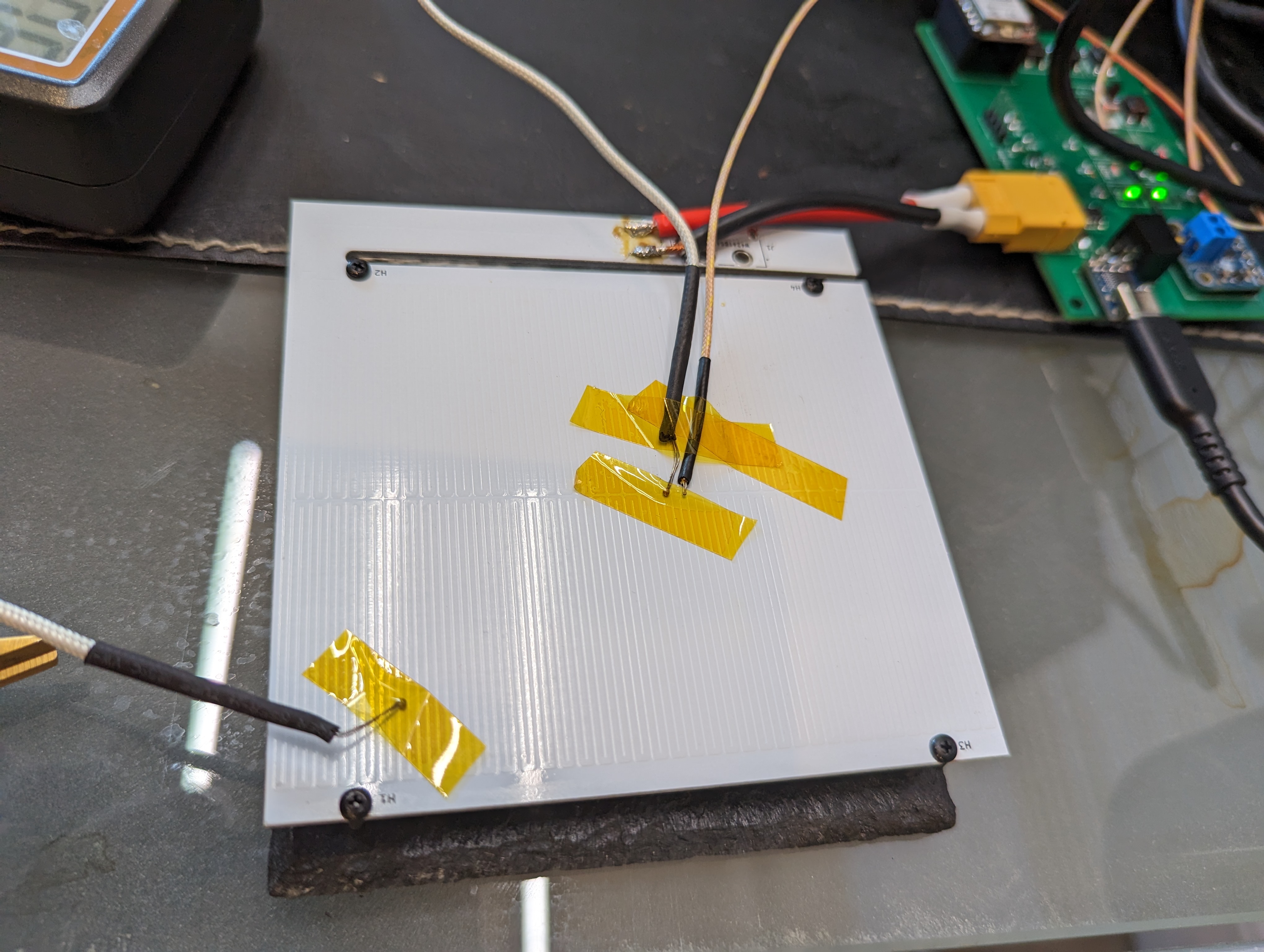
All my temperature sensors gave wildly different readings, even when co-located. I’m not sure why, but I do trust that the delta temperature measurements were ok since they were from the same instrument with two of the same probes, and they had the same readings when physically connected.
USBC-PD can deliver serious power, and its easily obtained with USB PD trigger boards.
Next Steps:
During testing, I learned what this type of soldering setup is really appropriate for, and what the capabilities of the heater are. I want to try some of this low temp solder, and I want to do some hot plate soldering to figure out how it feels, before going back to take another pass at the heater element. I suspect targeting an even lower heater resistance will allow me to hit 200C easily with the aluminum plate.
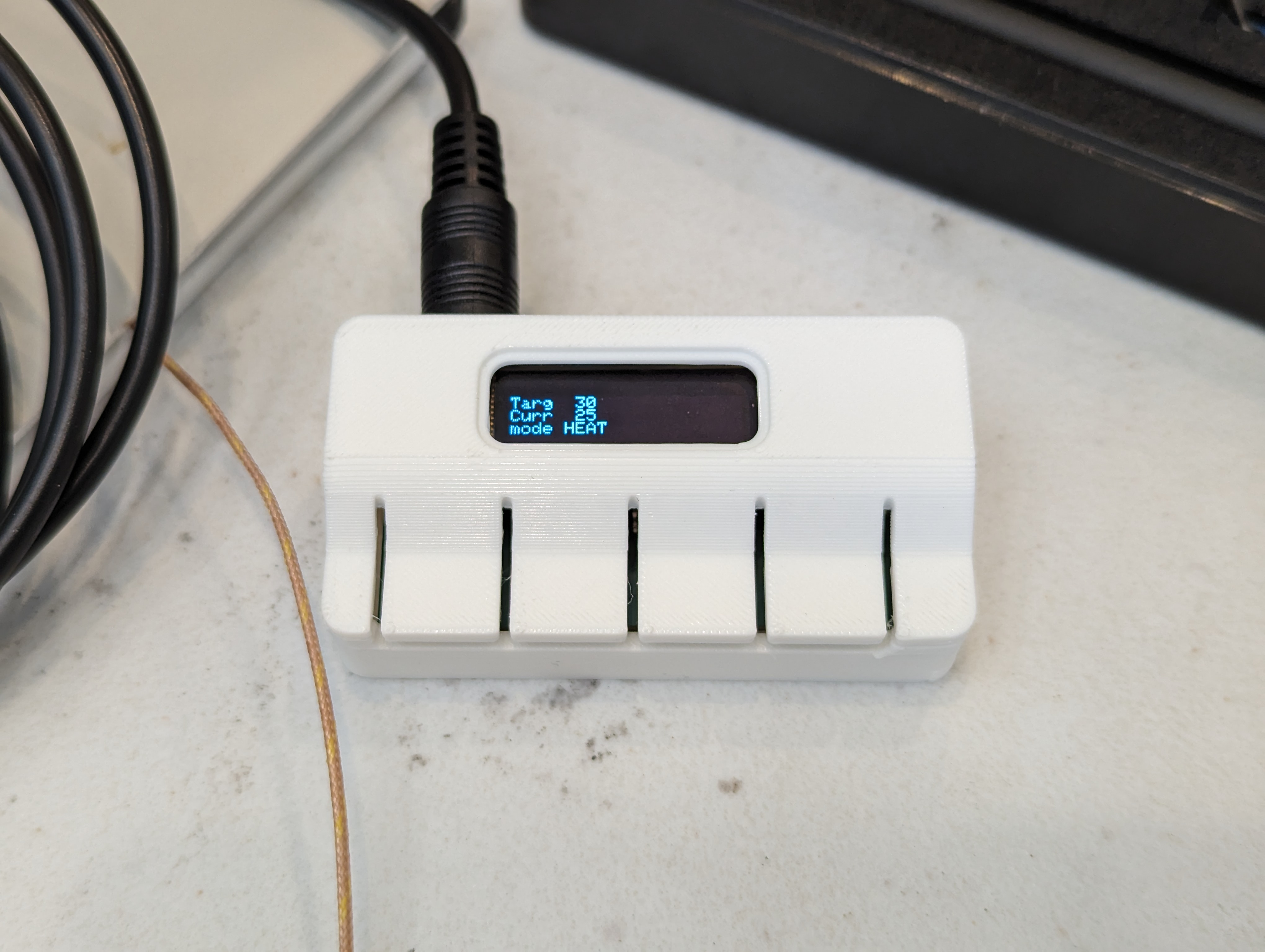
I also have some work to do on the UI (there is a screen- I just didn’t plug it in), and on the controls. If I find it useful, I will probably build an enclosure for it to protect the electronics and to make it easier to use.
The PCB heater for the hotplate obviously needs to be driven by something. I could have put more circuits on the heater board itself, but separating them has some advantages:
if the heater element is bad, or needs reconfiguration, it can be replaced
better opportunity for a heat break between the boards
opportunity to try different heater substrates or even different heaters/heater shapes
My goal for the hotplate is to keep it simple. I decided that I really probably need one profile at most, and a manual-temperature mode. I’d rather make that profile on the computer, instead of on the device, and be able to play it back from the device. I’d also rather get information back from the plate on the computer instead of a tiny display. Hopefully these simplifications will allow a hotplate to be up and running sooner rather than later.
Here is the architecture I came up with:
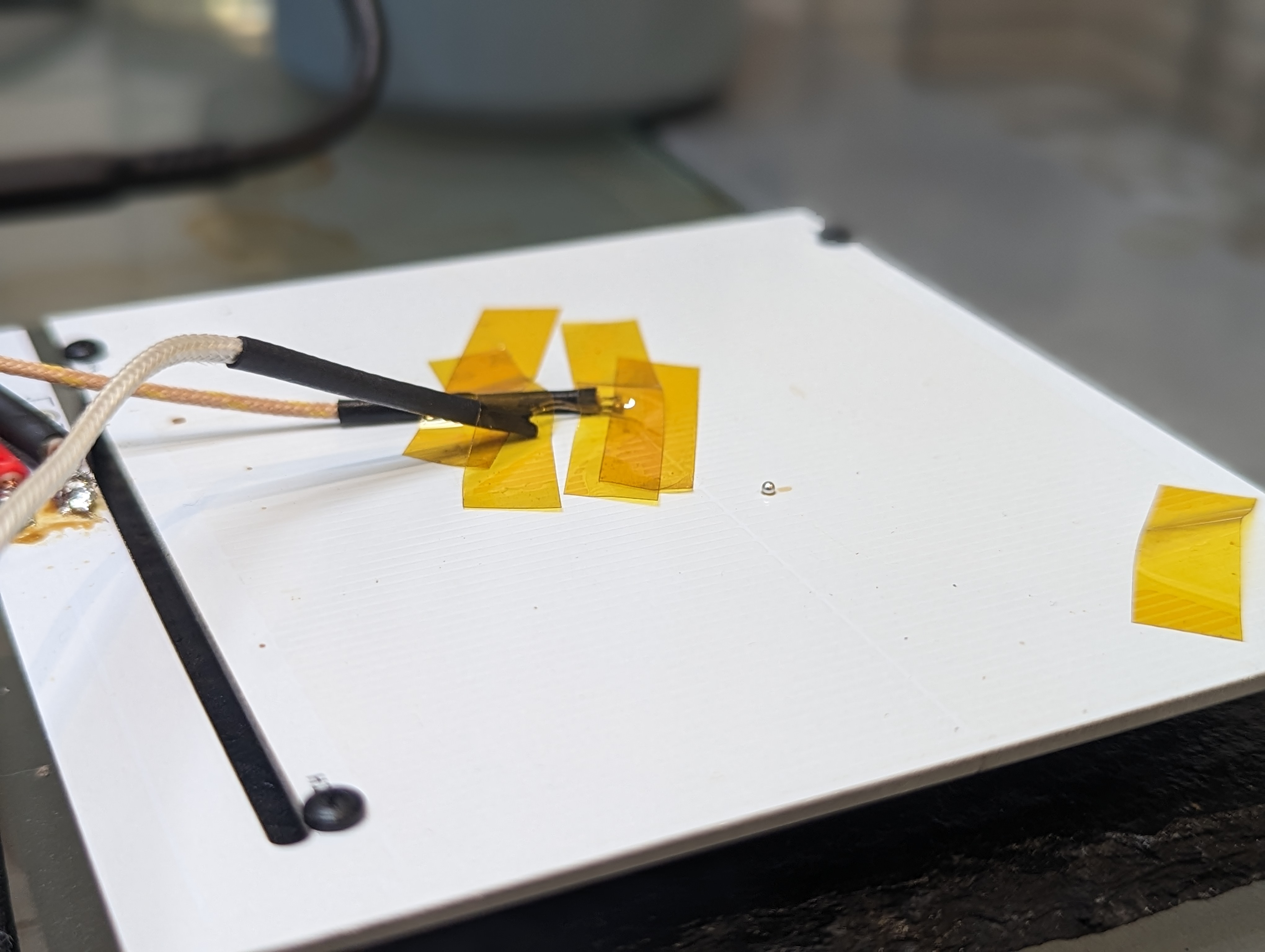
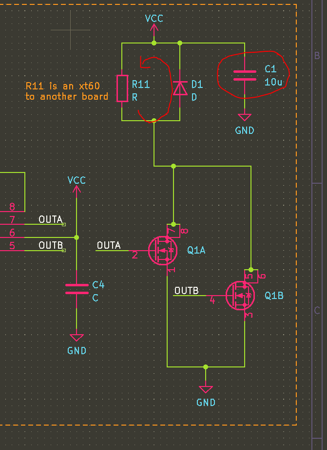
There are two usb C connections- one for programming the micro, and one for power, equipped with a USB PD “trigger” chip. My new favorite controller, the ESP32-C3 is in charge of the show (and native USB C). A single thermocouple is used for feedback, and an RTD is used as a safety cutoff- basically if it goes above some target temperature, the micro will no longer be able to drive the power FET. This won’t prevent the board from getting super hot, but it does provide a hardware safety against exceeding some set temperature if the controller spaces out…assuming the thermistor does not fall off.
Additionally there are indicators for PD power, DATA power, data transmission (heartbeat), heater power, and safety over temp, hot surface, mode, and (finally) a temperature readout. These are diagnostically useful, and they should satisfy my desire for a cool looking annunciator panel.
One annoying thing is that the ESP needs to be driven at 3v3 while the rest of the stuff is happy at 20V. While a cheap, integrated buck would be a neat solution, an LDO is so much cheaper. I decided to go with the buck, since I wanted to avoid burning extra power when operating near the 100W limit of the power supply.
The heater itself will be driven by a gate driver like the NCP81071B, which is 20V tolerant. 20V will just barely allow us to use something like the AOSD32334C, which is a dual N FET. Paralleling the FETS will reduce the RDSon to almost nothing- close to 10 mOhms.
The heater element here is represented by a resistor and an inductor- I expect the trace to have some very real inductance (100s of nH?), which will cause a large voltage spike when the FET turns off. This could easily exceed the 30VDS of the FET, and cause it to break down. The flyback diode will hopefully prevent this. Additionally, a capacitor Cbulk will be chosen to prevent over-drawing current from the power supply. At 20V, the 3.3 ohm heater will draw 6A, while the maximum allowed current is 5A. By PWMing this, the average current will be below or at 5A, but when the heater is on that current needs to come from somewhere- the bulk capacitance C.
To connect to the heater itself, I am using an XT60 connector. These are low-resistance and they seem easy to get, due to their use in drones.
Safety + Temperature Monitoring
There are a lot of ways making a big heater that is capable of destroying itself can go wrong. Ultimately this device falls under the category of things you should unplug if its not in use, and definitely not something to leave running unattended. However there are a few details I added as a nod to safety.
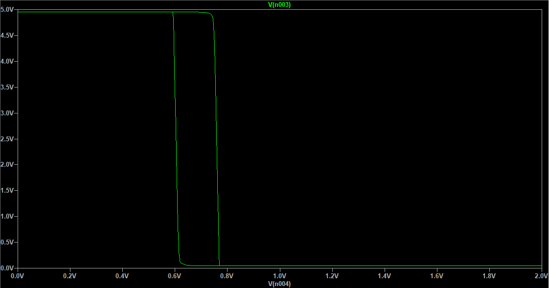
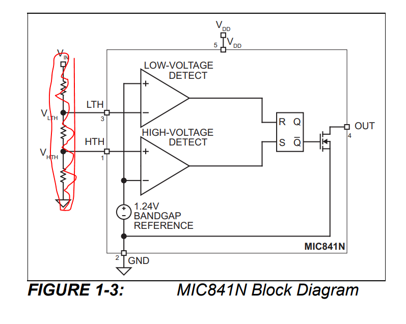
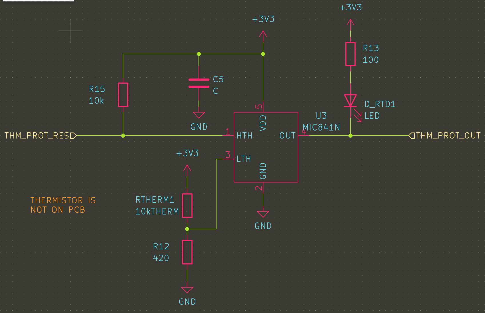
The first is a thermal trip based on the MIC841N The HTH input is fed by a NTC resistor divider that exceeds the 1.24V reference at about 200C. This SETs the latch, so the inverting output goes low, pulling down the enable pin of the fet driver. This is the case until either the whole circuit is reset (and the thermistor has cooled off) or until the reset line is pulled down by a button. Resetting while hot should result in an illegal state where ~Q is still 0.
Note: this circuit totally fails if Rtherm is removed, and it wont work if Rtherm gets disconnected from “the hot part”. If I wanted to add more logic, this could be resolved, e.g. inverting the logic of the resistor bridge. However, this is currently just a secondary protection. If it works nicely it can be refined later.
Temperature monitoring (for feedback and control) will be done with a thermistor dropped either onto the heater, or onto the target PCB. This allows for point control, near the stuff that you care about. For the time being, this will be made out of a MAX31850 thermocouple breakout that I have lying around from years ago.
Next Steps
With the heater and the controller designed, its time to get them made and then patiently wait for them to arrive!
I have started seeing a whole bunch of PCB hot plate builds, of varying success. I kind of want one now, since they seem very practical for one-off small PCBs, and most off the shelf solutions are quite large. However, I also want to improve on the state of the art of PCB heaters. These are useful for all kinds of stuff, from PCR machines to 3d printer hot plates.
There are a lot of challenges to overcome to make something that does not suck. Ideally, it could even be USB powered. Below are some calculations and considerations for making a pcb hot plate. You can see the WIP (scripts, pcbs, etc) on github.
PCBs are not a good material:
Using a PCB as a heater is not a new idea- however, in some ways, they are not good material candidates for high soldering temperatures:
The board will be at/above TG for a long time
solder mask/silk can discolor
could de-solder itself/the controller
repeated stress on copper tracks from board warping while heating
That said, several people have made them and they seem super-good-enough for this process.
Thermal Expansion
A lot of people worry about thermal expansion with pcb heaters- it makes sense because at the length and temperature scales that the heater will experience (100s mm, 200 C), real growth/shrinkage of the pcb will happen. With those temperatures and lengths, a FR-4 PCB will grow about .28 mm! An aluminum one will grow even more- .4mm! copper has a similar coefficient of linear expansion (alpha) as FR4, which means that the copper will need to stretch about .1mm/100mm of length. That is a strain of about .1%. That should be in the plastic deformation range for copper according to some stress strain curves I found, but it could cause cracking in more rigid parts of the assembly.
To further mitigate any expansion issues, I meandered the heaters on both sides, which should hopefully prevent pulling “straight” on any piece of copper. hopefully having a longer track (albeit, glued to the substrate) will help distribute the strain along the track- in the same way that a meandered track in a strain gauge rosette works.
In addition, I cut a slot between the hot part and the cold part, and put the connector thermally far away from the heater, while adding a lot of area for cooling. This should keep the connector from desoldering.
Low Voltage Efficiency Challenges:
A lot of these builds use lowish DC voltages to power the plate. This is not a great idea, because these things take a good chunk of power. Since the voltage is low, this drives up the current in order to deliver enough power. This results in losses in all the cables and connectors between the power supply and the heater.
As the impedance of your load approaches the impedance of the source of power, the power supply starts to eat a lot of power. I am considering all parasitic resistances here to be part of the “source” driving just the heating coil.
n is efficiency- as Rload gets to be about the same as Rsource, the efficiency will be about 50%- that means 50% of the power is going to get burned in whatever is supplying the power. This means that the rest of the circuit- connectors, fets, etc. need to be very low impedance compared to the load.
For example- to get a 100W heater at 12V, the Rload needs to be about 1.2 ohms This means that even a 100mOhm RDSon will drop the efficiency about 8%!
What would be ideal would to have the Rload to be greater than the R of everything else, by a lot. This is possible, but it comes with a catch- the current will be lower, and therefore, the power delivered to the heater will be low. Lets compare two cases, RL = 1 and RL=9, for Rs=1, and a source voltage of 10V that can output up to 5A.
Case
n, efficiency
Current (A)
Ptotal
Pheater
RL = 1
50%
5
50W
25W
RL = 9
90%
1
10W
9 W
An interesting (and not very important) aside is that for a particular heater power, and an infinitely powerful supply, there are usually two operating points for a given heater power. Check this out:
This gets turned into a very ulgy polynomial:
Lets look at a case where we claim Rsource = .5 ohms, V = 24v, Pload = 80 w.
If you crank this through the quadratic equation, (with some rounding) you will get R load of about 6 or .04 ohms. two very different resistances, but if you look at the same table you will see:
Case
n, efficiency
Current (A)
Ptotal
Pheater
RL= 6
92%
3.7
88W
80
RL = .04
7%
44A
1000W
80
yes- I rounded a lot but this is about right
Obviously, a heater with .04 ohms of resistance is impractical – the heater would be tiny (since the resistance has to be low), it would get SUPER hot because of the low thermal mass, and we would need to draw a kilowatt to use it.
Low Voltage Workarounds:
The good news is that the voltage does not need to be very high. Even a voltage of about 20-24 V (commonly available) is much better at delivering power than 12v.
Boosting to a higher voltage can help too. This won’t help as much as not having a low voltage at all, because the loss in the wiring/connectors in the low voltage section will still exist. However it could give more flexibility in the design or choice of heater elements. e.g. a 12W element that runs at 12V will have a resistance of 12 ohms (and a current of 1A). running this at 24V will result in a quadrupling of output power to 48W.
Ok, how much power do we need?
If we look at the existing hot plate examples, one figure of merit seems to be the steady state temperature at a given input voltage, and therefore power. My suspicion remains that connectors are eating a lot of power here, because the numbers do not add up. For example, at 3:10 in the hot plate V2 video we see the power supply is at 12V 7A, for a total input power of 84W. The temperature is 196C, with a room temp of about 25C. The heater diameter is .01 m2.
If the temperature is stable, that tells us energy in = energy out:
Using these numbers to back-solve for h, the convection coefficient, gives us about 44W/(m2k), which seems high. Given a similar delta T and the 70*50 area of the after earth board, the coefficient is about 10 W/m2k. These numbers seem high- I do not think all this power is getting delivered to the board, since a typical number for h is closer to 10-20 W/m2k for a pcb application. Its possible I am missing a few mm2 of area, or a lot of radiation or conduction, but these pcbs seem reasonably thermally isolated and appear to be in still air.
These designs come out to 5-10W/in2, or about 10kW/m2. I have seen a lot of heaters that claim to be 5-10W/in2, so that seems like a reasonable power to target.
Doing the math forwards (delta T of 175k, A= .01m2, h=25W/m2k), gives a desired wattage of 44W. I will aim to overshoot that, because it will reduce the heat-up time.
How fast does it need to get hot?
A good rate seems to be about 3C/sec, based on some reflow profiles. however, this rate needs to be done not only at the lower temperature, but near the top end of the reflow temperature- lets say 200c. This is important because if the heater is designed so that the max temperature is the reflow temperature, the heating rate will be slow as it approaches the max temp asymptotically.
drawing of typical newtonian heating
This is semi easy to estimate- we can make some assumptions, like that our heater is infinitely thin, massless, and is heating a plate that it is in very good contact with. the plate is also thin, so we don’t care about the gradient across it.
This basically says Temperature is equal to thermal mass * energy in an object. Taking the derivative with respect to time gives us a heating rate that depends on the heat into/out of the object. If we assume mostly convective cooling, and choose Qin, we can get a rate of temperature change. The delta T chosen tells us what the rate will be at a given temperature above ambient.
assuming a 1mm aluminum platen, with .01m2 of area, the volume is 1e-5 m3. with a density of 2.7e3 kg/m3, and a specific heat of 900 j/kgk, the platen has a thermal mass of about 73j/k.
for h=25 w/m2k a= .01 m2 dt=175, the convection term comes out to 43.75W (this is the same as the power needed to heat to this dt)
Tdot should be 3c/s,
so solving for Qin gives an power (at the heater) of about 100W. This is a rough SWAG, and it comes with the caveat that it will likely be even slower than that, due to delays in conducting that heat to the PCB.
Using USB C PD:
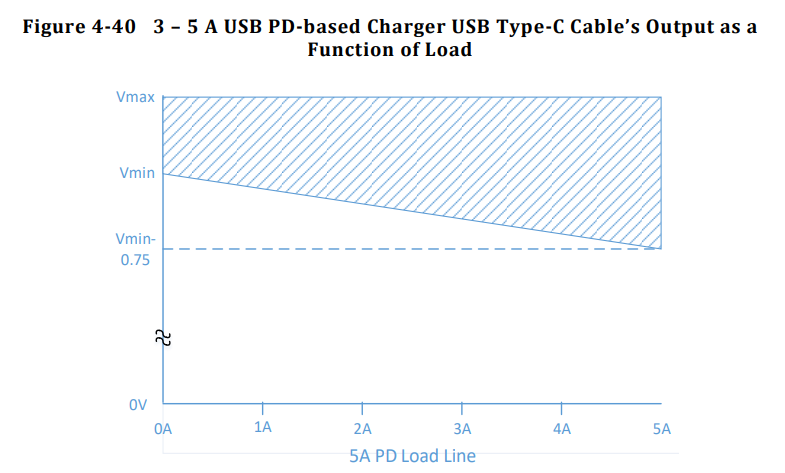
A USB C power delivery brick can, in theory, supply 100W. Really getting 100W out of a USB PD charger seems to be a bit of a stretch. There are tolerances on the actual voltage a given supply must provide, plus an allowable voltage drop (and power loss) in a to-spec USB C cable. Per the usb C R2.0 spec:
This Vmax and Vmin represent +/-5% of the allowable voltage. At 0A, there is no drop on the cable, but at 5A there is an allowable 750 mV drop. Interestingly, this drop is not symmetrical- only a 250 mV drop is allowed on the ground connection (even though it should have the same current flowing through it). This voltage drop at 5A means that a USB cable is allowed to burn about 3.75W.
This means the worst case voltage to come out of a 100W PD supply and cable at 5A is really 18.25 V, which is really closer to 91W. However, as much as 20.25V can be delivered at 5A, for 101.25W (with an ideal 0 ohm cable).
This means to get the full power out of the lower allowable voltage chargers, (18.25V), the heater resistance will need to be 3.65 ohms. however, that will draw too much current on the high side. the solution seems to be to cater to the lowest voltage, and then PWM the heater (which I will do anyway) so that it does not exceed the average current draw for higher voltage/lower resistance supplies. Designing around the higher voltage supplies will result in a under-powered design, since we will not get the full 5A at lower resistances.
Additionally, there needs to be some allowance for other resistive circuit elements, e.g. the switching FET, solder joints etc. Estimating a few 300 milliohms for those seems ok, so so the real target heater resistance should be about 3.3 ohms at room temperature.
Resistance Temperature Sensitivity:
Resistance of materials increases with temperature. Copper increases about .0039 ohms per degree ohm. With a delta T of 175K, and a target resistance of 3.3 ohms, this means that the resistance will increase by 2.2 ohms! This means that at higher temperatures the maximum output will be closer to 72W.
It is easy to calculate what original resistance would give us 3.3 ohms at 200C- this turns out to be about 2 ohms. However, the bulk capacitance required to smooth out the ripple at 10kHz is about 1000uF, which is expensive to implement. Using an electrolytic capacitors incurs a pretty steep power loss in parasitic resistance, and ceramic capacitors are too expensive for the design. I will stick with 3.3 ohms for the design, and just loose some power generation at higher temperatures.
Heater Design Math:
What follows is a detailed design of the heater traces. An important concept is sheet resistance- this is the concept that the resistance of any square of material in a homogeneous sheet has the same resistance. 1 oz copper has a sheet resistance of about .5 mOhms, per square.
As we know from our previous calculations, the resistance of the heater should be about 3.3 ohms. We can use this equation to get the number of squares:
From this I calculated that the number of squares needed is 6600. This means the trace for the heater (if its made of 1 oz copper) to be 6600x longer than the width.
I want the heater to be about 100×100 mm, or less. This will give us an area of about .01m2, which was used in the calculations above for heat transfer. Ideally, the heater would be a little smaller, in order to hedge on the side of performance. Another practical consideration is putting the power terminals next to each other- this will minimize the length change between them when hot, and it will make the wires going to the heater short (preventing a wire run from another edge or corner of the board).
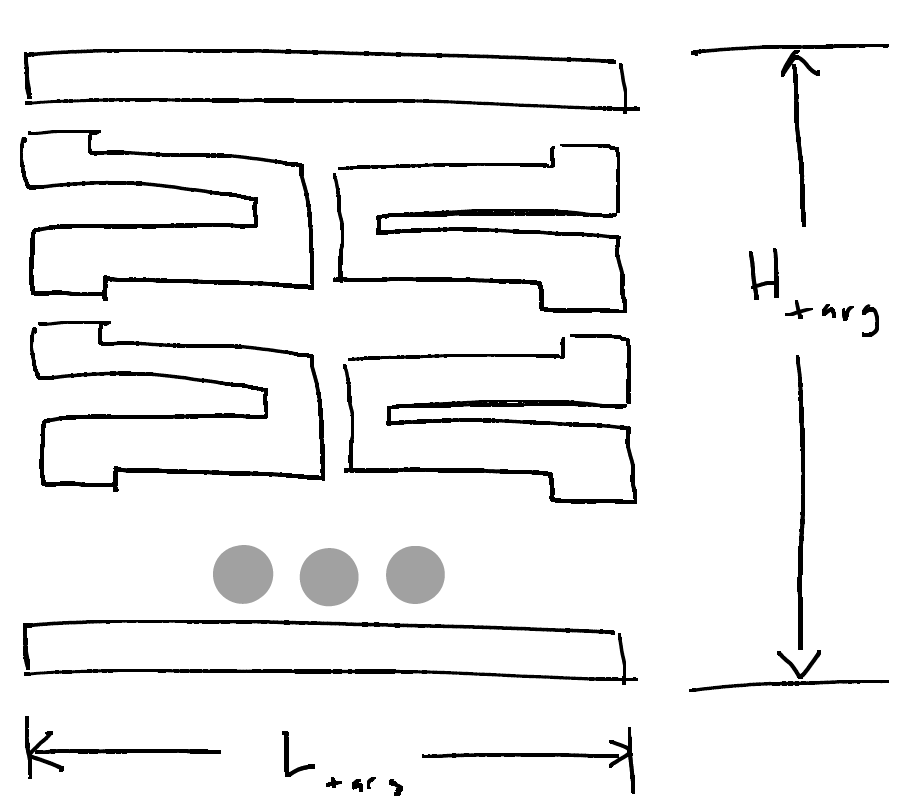
In order to meet these requirements, I wanted a rectangular pattern that would fill in the heater rectangle. I opted for what I decided would be called a double zig-zag, which can be cut anywhere on the perimeter so that the power terminals are next to each other. The extra long trace should also help prevent from stretching the copper under thermal expansion, since the whole pattern should act like a spring.
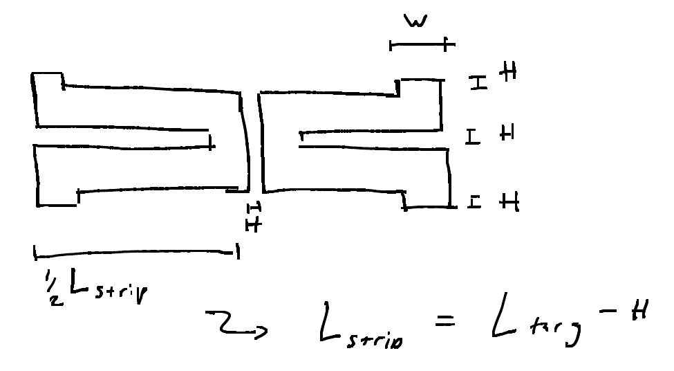
This drawing shows the units broken down- two long bars Ltarg long of width W, and several units that would each be connected to each other. Each unit has these dimensions:
The ideal distance between the tracks, H, should be very small, because it will result in more coverage of the board in heater tracks, and therefore more even heating. I chose to start H at about 6 mil/.16mm. H needs to be varied so that the total number of units, N, is an integer. having a half-unit means that the spacing will be off or that it will not be possible to terminate the pattern properly. The next thing to do is to come up with a couple relationships for the geometry of the pattern. The first is that the pattern must be a certain number of squares long. This sum is the top and bottom width full length bars plus N units * squares per unit. The Number of units, N, also has to be equal to the target height of the units (Htarg – 2w) divided by the unit height. Here h is the spacing between units, and H is Htarget.
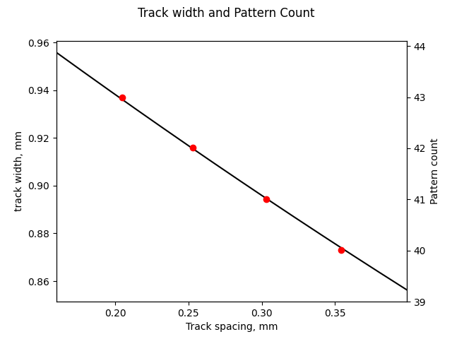
These first two expressions combine, after some work, into this ugly polynomial. we can now input an h, spacing between traces, and get out w. w allows for computation of N, the total number of units, which must be an integer to be valid. see plot below to compare red dots (N) to track width (mm) vs spacing, h (mm), as the spacing is increased.
With this computed, it is easy to choose the best outcome, where the track thickness is maximized, and spacing is minimized, to create an evenly heated area.
Final design:
I decided that the heater dimension should be 100×76, since it is a little smaller than .01m2, which should give better performance at 100W. It is also a reasonable size for most PCBs I would make and under the price break dimensions for aluminum PCB.
Since the pattern can’t go all the way to the edge, and because the mounting is somewhat TBD, I decided to subtract a 1mm border on the long (100mm) dimension and add 4mm border on the short dimension. This makes the final dimensions for the board 100×100 (including connector), and the pattern dimensions 98×78 mm.
For a target track resistance of 3.3 ohms, the calculator reports that the width should be .996 mm, with .267 mm spacing, and 38 repeats.
Kicad Plugin
Of course drawing this trace is tedious and difficult to get right. A plugin was designed to draw the trace meander. Details can be found on git.
Next Steps:
The next thing to do is to ship the design off to be fabbed. I’m planning on trying both FR4 and aluminum substrate PCBs. FR4 has the advantage of having a similar linear expansion coefficient as copper, and being an ok insulator. Aluminum on the other hand, is possibly more rigid than FR4, and is a good conductor/heat spreader- this would be good to prevent heat buildup in any one trace. I will also need a controller for the heater, with a micro, a sensor for feedback, etc (post coming soon).
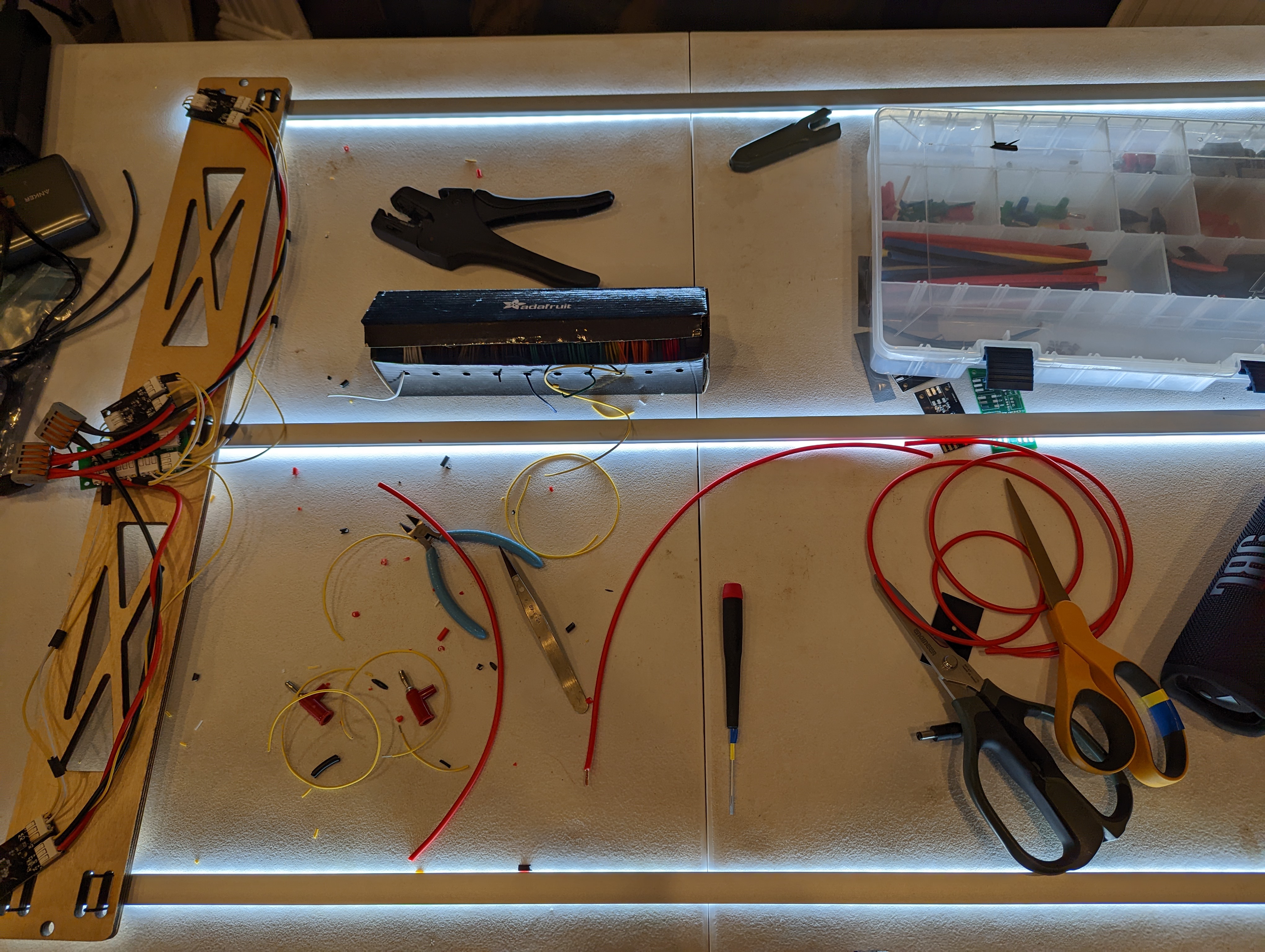
In my last post, I discussed the basic requirements and layout of my lamp – I wanted it to be able to control the color temperature and brightness, and I wanted it to be really bright. I experimented with a single strip, and detailed how the control board would work. If you want to try to build your own, the code/boards are here, although it is not very well documented.
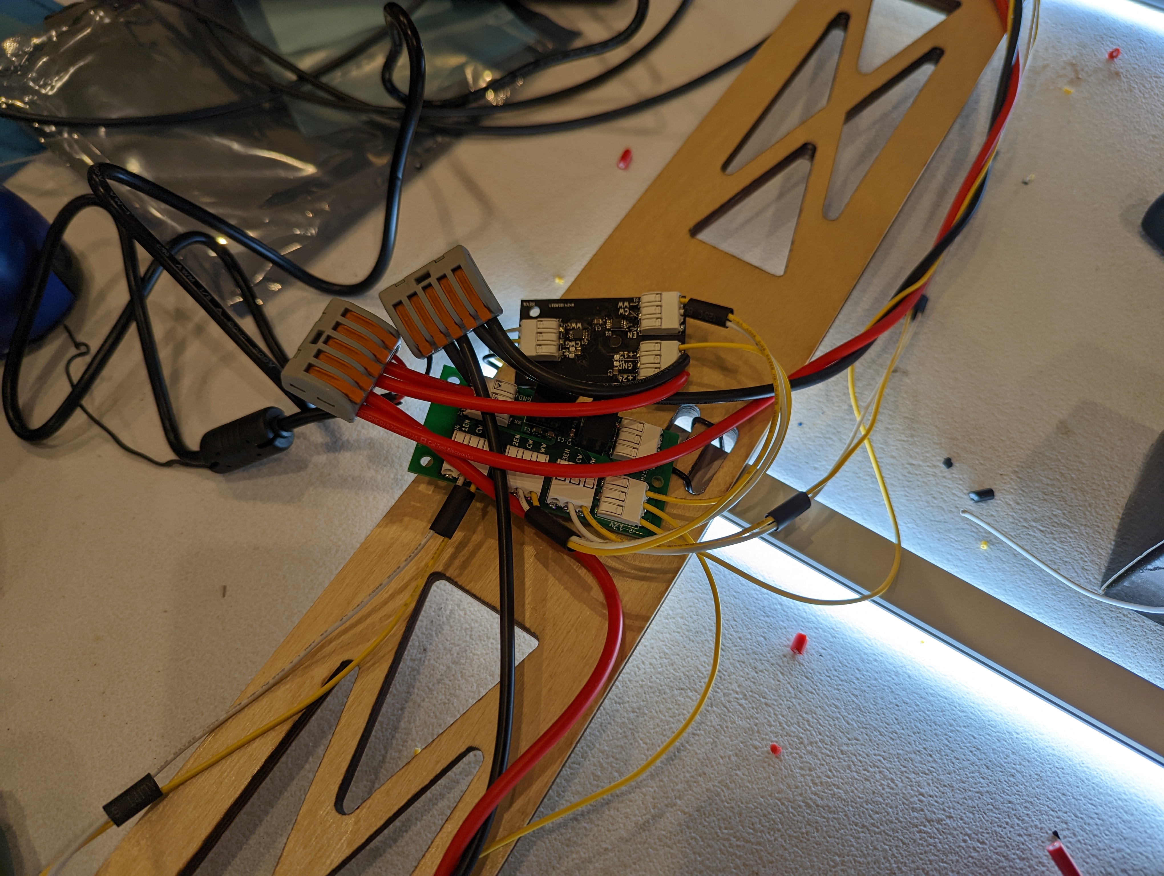
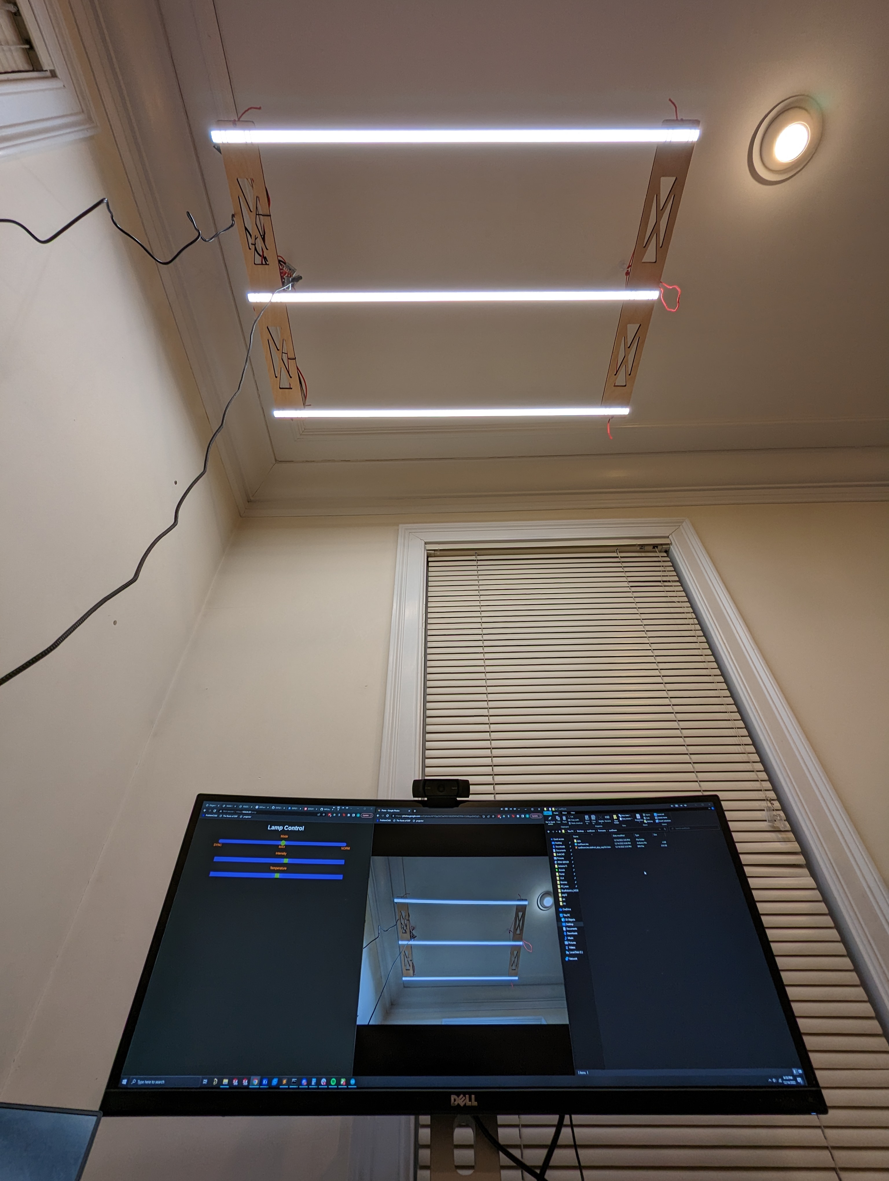
Here is the control board all wired up. It packs an ESP32-C3, because I had one on hand, and because connectivity is important for this project. In addition to manual over-the-air control, I want to be able to put the lamp onto a simulated daytime color temperature loop- a real-life version of f.lux, which turns up the warm temperature light on your display as the day progresses. I also would like to add a way to sync it to some kind of live color temperature data.
This wiring leaves a lot to be desired- this is because the boards and mechanical assembly were developed at different times, and the mechanical side of things ended up going to “plan b” aka laser cutting. It might be worth revisiting in the future, especially because a lot of ports/connectors ended up unused. For now, I am just happy to have a lamp.
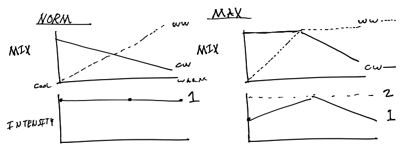
Here is the control page that the lamp serves up. It lets you choose a mode: SYNC, MAX, or NORM.
Norm is a smooth light intensity with changing color temperature- the output never exceeds the brightness of having all warm or all cool lights on, so when the temperature is “balanced” the output is 50% brightness warm, 50% brightness cool.
Max allows for the overall maximum light intensity to vary, but keeps the mix “smooth”. So at full warm, 100% intensity, the brightness of the warm strip is 100%, and at “balanced” temperature, 100% intensity, the output is 100% warm 100% cool.
SYNC will take over both intensity and temperature and to create a profile that mirrors a day, which is still TBD- to be developed. There are many ways this could be implemented, from having the lamp look up the weather/sunrise/sunset, to building a weather station, to having a server on a main home automation controller that tells the lamp what to do. Its also not totally clear to me what the ideal profile would be- for example I would like to have nice bright light, even in the early evening, so I don’t want it to totally follow the real “day” profile.
Mechanical Notes + Details
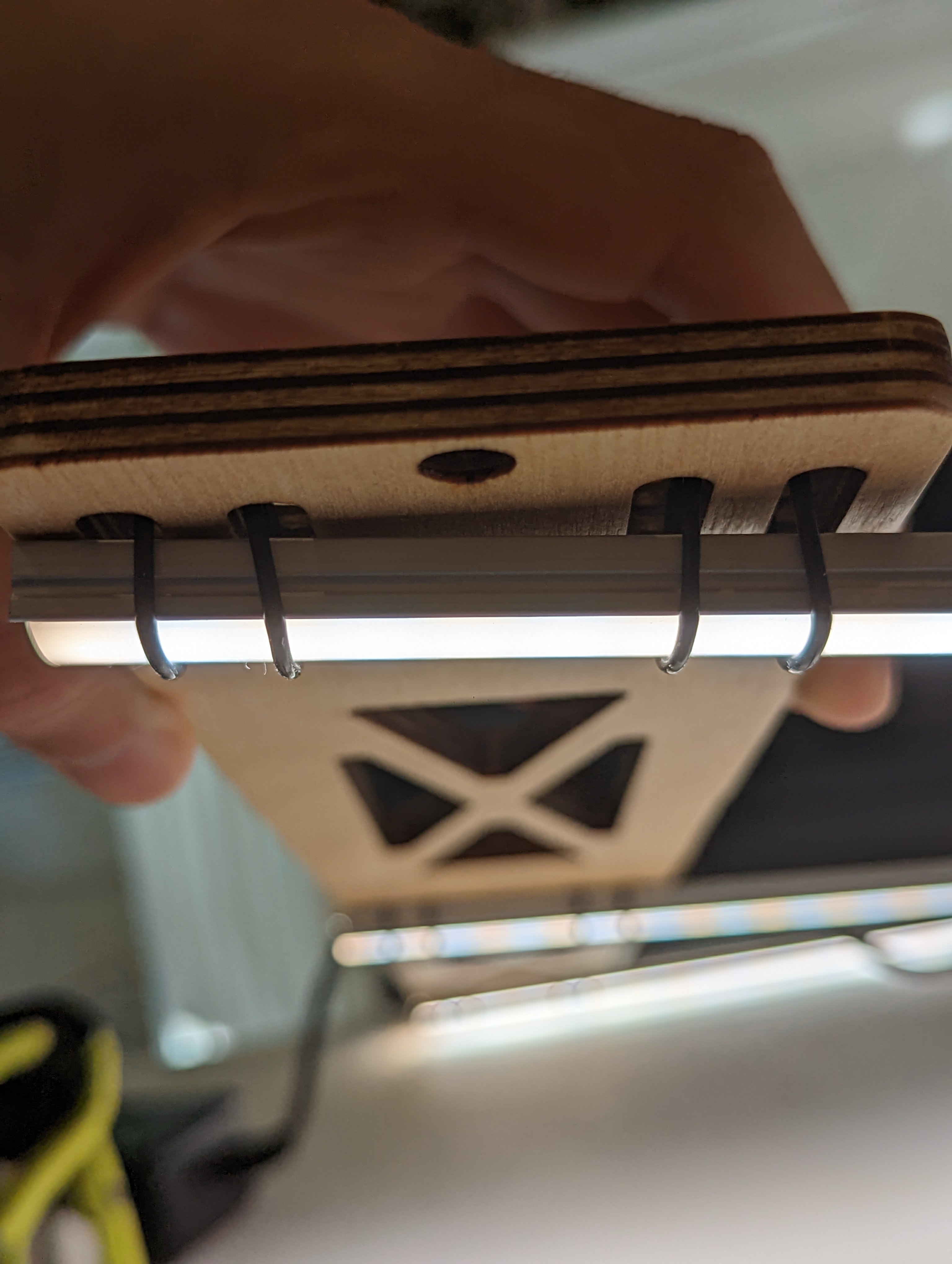
This lamp, despite not achieving one of my crazy tensegrity ideas, fancy woodworking concepts, or brass-pipe dreams, does use one of my favorite tricks: using orings as precision rubber bands. The LED channels are very thin, and therefore fairly hard to attach to with screws. They are meant to be mounted with supplied clips, but I didn’t feel great with those overhead, since they are not closed on the bottom.
Instead of clips, I used the aforementioned fancy rubber bands, with two per side (four total) per LED channel. This means that if one breaks, I will have time to notice and replace it. Since they are flexible, the overall alignment of the strips matters less and the hole placement does not need to be spot on. They are also very thin, so they don’t block light.
Another interesting fabrication note is how I removed the scorching from the laser cut cross-bars. These were completely covered in soot as-cut. Usually cleanup of parts like this is annoying and time consuming because the soot is ingrained in the plys of the wood. This means the parts need to be sanded back significantly in order to remove the soot, causing the overall shape of the part to change. In this case I had access to a media blasting cabinet- a light blast with glass media removed most of the scorched material, saving time and preserving the shape (and sanity).
Done?
This is the kind of project that could go on forever, but for now I will enjoy having a nice lamp. Here is a short list of improvements for “someday”:
use websockets for more responsive control of the lamp
make lamp status persistent
find a nicer looking power supply
add a setup page/wifi STAtion mode as a fallback in case it can’t get on the network
finish daylight color tracking/sync mode
redo the PCB +other components to make it less of a noodly mess
add a display (of some sort) to show the IP address
use the neopixel on the dev board to indicate connection status