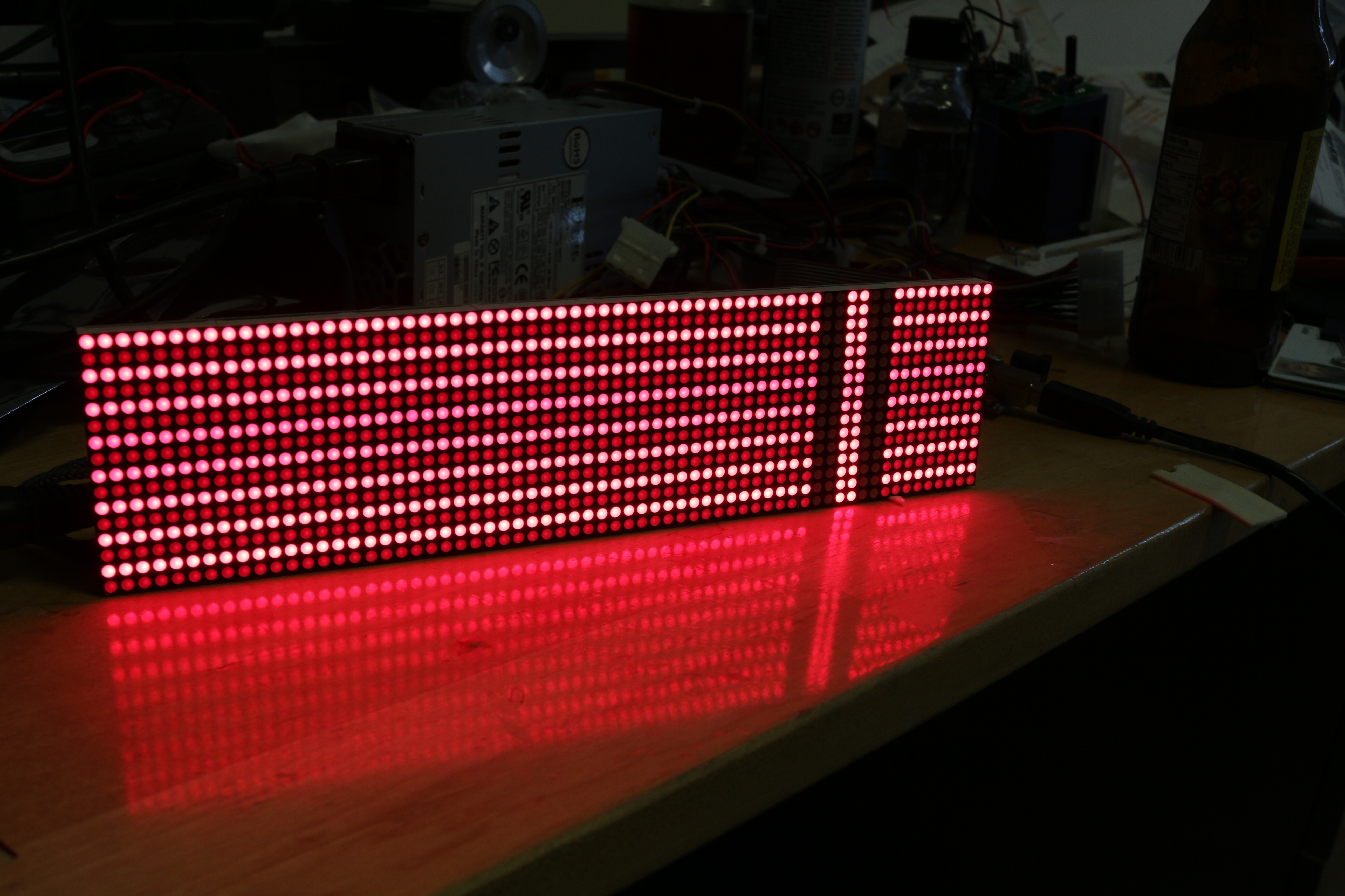
They look pretty good…
I am working on a project for someone, which I was encouraged to post here. The goal is to explore making big led panel displays available as a module for new wireless development platform (the tessel). As part of my assignment, I need to asses the viability and quality of several LED panels. I will be starting with the LDP-6416 from Embedded Adventures.
The display is 64 lines “long” and 16 lines “high”. Only one row of 64 LEDs can be on a time- this means to create a persistent display, the rows need to be enabled over and over very quickly. Additionally, the LED display is relatively “dumb”, and the line needs to be shifted in each time before it is displayed. This means that you put some data on the R1 and G1 pins, then you pulse a pin to put that data into the LED driver register. The reasons behind this are covered in the electronics tear-down below.
The result is that the person developing on the board needs to be protected from having to devote a lot of resources to flash the board over and over, because that would take a lot of memory. Also, there needs to be some way of scrolling the display, since that is a pretty common task that should not require the image to be shifted on the main processor, then retransmitted to the panel module and re-displayed over and over again. My goal was to evaluate if functions like scroll_text(‘ASDF’); and static_text(‘ASDF’) would look good and be easy to implement.
It turns out to be pretty easy to scroll text if you store your data thoughtfully. My experience with the code is below, followed by an electronics teardown of the module, and a short second on reducing ghosting and flickering. At the very bottom are a few caveats and suggestions if you want to use the code. If you want to run it, check the caveats. the code is available on github, as well as being pasted below.
CODE
There were three main revisions of the code, which got faster and faster. The speed had to increase to reduce flicker due to refreshing of lines. The takeaways are: use the right type of variable, and put pins you want to change at the same time on the same PORT.
The metrics for “goodness” of the code were how much program storage and dynamic storage it took up, and how much the display flickered. The dominant function in terms of time-usage is the function that loads the image into the row, so that is what is scrutinized in these attempts. The code was compiled with the -O3 (optimize for speed) optimization command passed to the compiler, so some of the code blowup in the first two functions may be because of in-line arguments etc. Also, only the data for the image and the data for the data driving were compiled- no extra loops or functions.
The latest code is available on github, complete with comments
Naive Attempt: 1484 byte program memory, 521 byte dynamic memory, flickery
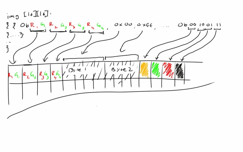
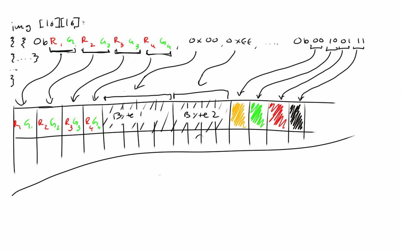
Each byte contains four pixels
My normal approach is to try the easiest way to do something first- just to check things out, and to make sure things are hooked up right. Sometimes it even works well enough to use as a prototype. In this case it would have worked if the arduino were about twice as fast, but it was still a good way to start seeing how the panel worked.
The “image” data was stored as an “int image[16][16]={{0xff,0x55..},…}”. Each alternating bit was a green, then red value for a pixel. This turns out to be a stupid way to store the image, but it does work. The issues with this image storage are that ints are 16-bit in this implementation, and I only used up to 8 bits of them. byte image[16][16] is the way to go if you want to store 8 bit values.
The code was also pretty bad. The wiring was such that the pins that were clocking the signal out to the LEDs were on different PORTs. Here is the function:
void noob_line(int line){
for(int k=0; k<16; k++)
{
for(int j=3; j>=0; j–)
{
digitalWrite(0,bmp[line][k]&(0b1<<j*2)>>j*2);
digitalWrite(1,bmp[line][k]&(0b10<<j*2)>>j*2);
digitalWrite(2,LOW);
digitalWrite(2,HIGH);
}
}
digitalWrite(13,HIGH);
digitalWrite(13,LOW);
}
On the surface this doesn’t seem too bad- it is basically just doing two writes, clocking in the data, and then latching it at the end. The thing that kills this function and causes the flicker is actually digialWrite. It seems innocent enough, but digitalWrite actually takes quite a bit of time. One guy clocked it at 4.75us, which is around 40 instructions. Round that up to 5us, see that there are 4 calls, and the loop runs 64 times, and you will notice that it is 1.3 miliseconds! That means the whole screen is only updating 50 times a second. With no fine grain or motion blur, like a movie has, this is pretty apparent. That doesn’t take into account the logic operations and retrieving the data form the image, but its not a good number to start with.
Proof Attempt: 1120 byte program memory, 265 byte dynamic memory, no flicker

flckr-less. Showing off some of the colors with a silly test pattern
At this point, I just wanted to make sure that the display would work without flicker. This one went way faster and used much less program memory to store the image, since the type was set to byte instead of int. I could have used half as many ints instead, and taken the same amount of memory, but there is something appealing and fast about using 8 bit numbers on an 8 bit micro.
This loop went a lot faster because I wrote directly to the PORT, and I put all the pins on the same PORT. I didn’t clock the function since it was not flickering, but an easy check would be to use an oscilloscope on the latch line.
Here is the code:
void send_line(byte line){
for(int k=0; k<16; k++)
{
{
for(int j=3; j>=0; j–)
{
PORTD =0b11111000 | ((bmp[line][k] & (0b11<<j*2))>>j*2); //access some memory
PORTD|=0b00000100;
}
}
}
digitalWrite(13,HIGH);
digitalWrite(13,LOW);
}
As you can see, the four digital writes have been replaced. The nice thing is the boolean functions are all acting on 8 bit registers, so each one should take about one operation. Thee are five of them, which even with 200% overhead for getting variables from memory only takes 63 microseconds. The estimated time for the function to run is then 40 microseconds, or about the amount of time it takes to run 10 digitalWrites. If I wanted to go faster, I could even use a PORT write instead of digitalWrite to latch the data.
Anyway, this was MUCH faster. But still, there was no good way to scroll the data. The obvious approach to scrolling is not to rewrite the entire image, but just to shift it over. However, since the data was stored in bytes, there was not an easy way to index a shift of one pixel, because of the inner loop always runs four times. Since the data was indexed by bytes that coded for four pixels, it was easy to scroll by four, but not by one, two, or three pixels.
Wise Shift: 740 bytes program memory, 137 bytes dynamic memory, no flicker

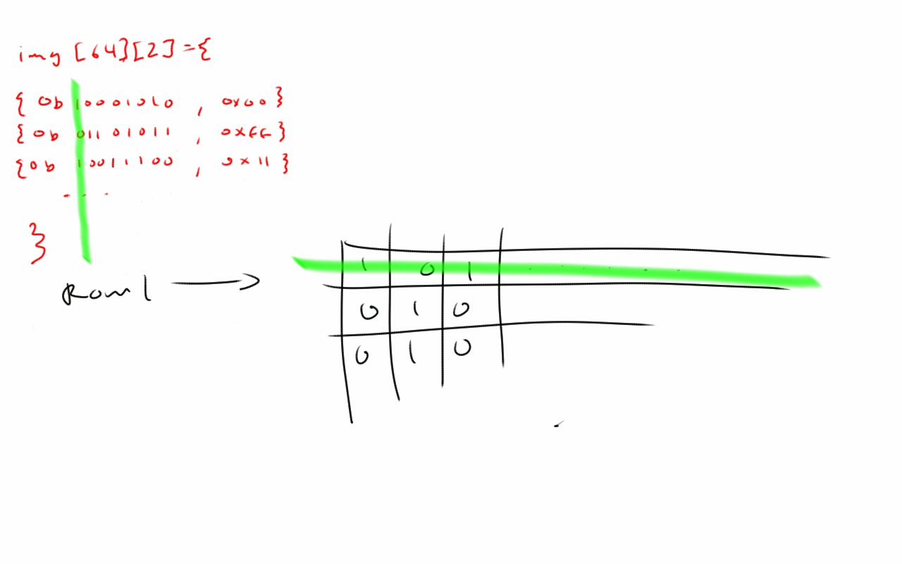
now each bit of a 64 bit row is addressable individually
I called this function wise_line since the data structure used to store the image was wiser. To be efficient, I packed the data into bytes just like before, but to be wiser, I made the two matrices of [64][2] instead of [16][16]. This means that imj[0,1,2…63][0] gives you the top 8 pixels rows, and imj[0,1,2…63][1] gives you the bottom 8. Now if i want a 64-pixel long row, I can just ask for imj[0…64][0] and mask it with the correct row.
Same amount of data, but much easier to deal with! Now I can iterate down a column and start and stop at any point. This makes scrolling easy!
void wise_line(byte line,byte shift)
{
for(byte i=shift; i<64; i++) //print everything from shift onwards
{
PORTD =0b11111010 | ((img[i][line>>7]&(0b1<<(line&0b111)))>>(line&0b111));
PORTD|=0b00000100;
}
for(byte i=0; i<shift; i++) //print the rest of the picture
{
PORTD =0b11111010 | ((img[i][line>>7]&(0b1<<(line&0b111)))>>(line&0b111));
PORTD|=0b00000100;
}
PORTB|=0b00010000;
PORTB&=0b11101111;
}
Now to scroll, all I have to do is print img[shift,shift+1…63][n], then print img[0,1…shift][n]. I decided that byte line would hold all of the data for what line you to print, specifically:
byte: | 7: upper/lower display | 6-3 empty | 2-0 column mask |
so line>>7 tells you if you want image[n][1] or image[n][0], and line&0b111 tells you what part of the byte is the correct row. The nice thing is that to display a given row of pixels, you don’t have to change any index except how far down the row you are- the top/bottom and mask information is the same.
The result is that scrolling and other effects involving shifting images are easy, and the code is much, much smaller and faster. Over the three iterations, the program memory only dropped by about 50%, and the dynamic memory dropped by about 75%. The main memory gains were made by using bytes instead of ints, which are half as big, and replacing slow arduino function calls with faster PORT writes and a little bit-math.
ELECTRICAL
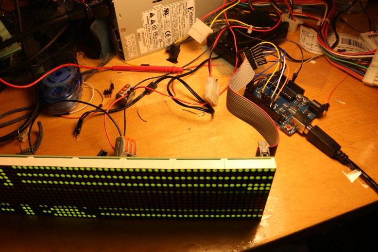
Wires. Everywhere.
The panel itself is pretty easy to hook up and use. Power is needed in abundance to drive the panel, but it only needs one line lit at a time, and that line can be PWMed on the ~enable pin to reduce average current draw. Fully lit, the datasheet says it will draw 4A a row, so a 5V 5A power supply seems like it would do the trick with a spare amp- a tiny portion of which could be used to power a microcontroller.
There are 10 connections that are important, but 16 pins in the header, so it is not nearly as bad as it seems at first. Since it is a test setup, I just jammed some male-male headers into the connector. The important lines are:
- ground
- ~enable
- latch
- shift
- ~Green data
- ~Red data
- A, the first bit of the row selector
- B, the second bit of the row selector
- C, the third bit of the row selector
- D, the fourth bit of the row selector
The arduino pin numbering for these pins is provided in the code on github. and copied at the bottom of the document.

The backside of the board.
The chips on the board are the usual suspects- lots of 74 series logic, and some FETs.
There are 8 FDS4953 FET packages, on the board, each containing two transistors. There are two SM74HC138D decoder/demultiplexers, and 16 74hc595 shift registers. The LED panels look like the typical sort which can only actually have one row on at a time anyway.
With 8 FET packages at two FETs per package, you can imagine pretty much exactly what is going on. Each FET powers a row of LEDS. Using a continuity tester reveals that the top and bottom decoders are connected to the ABCD row select pins on the control header, so those pins get demultiplexed and used to turn on the FETs, which are each connected to a row pin on each of the LED panels. So the flow looks like this:
ABCD pins–>74HC138D–>FDS4953–> all of the H# pins on the top panel
The H# (where # can be 1-8) turn on one row of each of the panels on one side of the board.
So that is power. The logic is pretty simple as well, since it is just a bunch of chained shift registers. One chain of 8 registers controls each color, and turns on all the pixels in a column. The FET then selects the row, and the two output a single line.
And there you have it- a big, cheap LED driver board. The last interesting thing here is that it was not designed by Embedded Electronics- I think I was shipped an old rev. of the board, because it lacks the screw terminals, chip position, and silk of the picture on their website. This board is copyrighted 2013 by linsn, which looks like an LED panel supplier.
Increasing Brightness, Reducing Flicker and Ghosting

Ghosting is noticeable between rows here in this picutre. *(cylon noises)*
Flicker is caused by going too slow, and Ghosting is caused by having the enable on before the data is shifted in. In my first, slow attempts I had a line like:
analogWrite(EN,1); //keep EN low most of the time, flash it at ~500hz
This made the display ghost, because the LEDS would light up as the data was propagated across the registers. It would also cause flickering because the code was slow. One way to mitigate flickering if your code is too slow is to display lines in a random fashion- it can be the same pattern every time, but if you refresh lines next to one another it can cause a traveling wave pattern of flickering if the code is not running smoothly. This goes for anything that has a consistent direction, including refreshes from the outside in or inside out.
Once the code was much faster, I would manually enable/disable EN after the line was written. This causes a dim display because the code loops back around and pushes the next line immediately, like so:
void loop() {
disable_display();
push_line();
enable_display();
}
Inevitably, it would spend most of the time doing the push_line() command, and during that time the display was off. The fix to this is to write:
void loop() {
disable_display();
push_line();
enable_display();
delayMicroseconds(a_few_us);
}
to allow the panel to shine. This value can be tweaked up to the point where you start to see flickering, and it will make the display brighter.
Caveats and Suggestions for Implementation:
So you want to scroll some pixels. The only bugs right now are a tiny pause when the shift value is reset, but this could be fixed with some clever use of binary math. It is only noticeable if the scrolling is fast.
This code was written at max speed- therefore some lines are somewhat obfuscated. They have been commented to try to de-obfuscate them, but I admit they could still be confusing.
You may need to change the delay value, discussed above.
There is also a pretty big problem in loading the data, since you have to generate the map by hand at the moment. you could write some python that pushes it to the arduino, or a gui for generating maps.
Lastly, the scrolling function is pretty boss. You could change the code to have a longer img matrix, like a [128][2] and have a longer scrolling message, or you could save sprites and make an animation…there is a lot of room left on the arduino!
CODE PASTE!
/*
LED driver software for LDP-6416
Written by Avery Louie for Ryan Hurst
*/
//defines used on old versions of code, still useful for wiring reference
//all these pins live on PORT D, D0-3
#define RD 0
#define GR 1
#define S 2
#define EN 3
//all these pins live on PORT B
#define A 8
#define B 9
#define C 10
#define D 11
#define L 13
//the “image” for the static test using send_line and noob_line
byte bmp[16][16]={
{0x00,0x00,0x00,0x00,0x00,0x00,0x00,0x00,0x00,0x00,0x00,0x00,0x00,0x00,0x00,0x00},
{0xAA,0xAA,0xAA,0xAA,0xAA,0xAA,0xAA,0xAA,0x55,0x55,0x55,0x55,0x55,0x55,0x55,0x55},
{0x55,0x55,0x55,0x55,0x55,0x55,0x55,0x55,0xAA,0xAA,0xAA,0xAA,0xAA,0xAA,0xAA,0xAA},
{0x00,0xff,0x55,0xAA,0x00,0x10,0x00,0x00,0x00,0x00,0x00,0x00,0x00,0x00,0x00,0x00},
{0x00,0xff,0x55,0xAA,0x00,0x01,0x00,0x00,0x00,0x00,0x00,0x00,0x00,0x00,0x00,0x01},
{0x00,0xff,0x55,0xAA,0x00,0x00,0x10,0x00,0x00,0x00,0x00,0x00,0x00,0x00,0x00,0x00},
{0x00,0xff,0x55,0xAA,0x00,0x00,0x01,0x00,0x00,0x00,0x00,0x00,0x00,0x00,0x00,0x01},
{0x00,0xff,0x55,0xAA,0x00,0x00,0x00,0x00,0x00,0x00,0x00,0x00,0x00,0x00,0x00,0x00},
{0x00,0xff,0x55,0xAA,0x00,0xFF,0x00,0xFF,0x40,0x00,0x00,0x00,0x00,0x00,0x00,0x01},
{0x00,0xff,0x55,0xAA,0x00,0x00,0x00,0x00,0x00,0x00,0x00,0x00,0x00,0x00,0x00,0x00},
{0x00,0xff,0x55,0xAA,0x00,0x00,0x00,0x00,0x50,0x00,0x00,0x00,0x00,0x00,0x00,0x01},
{0x00,0xff,0x55,0xAA,0x00,0x00,0x00,0x00,0x70,0x50,0x00,0x00,0x00,0x00,0x00,0x00},
{0x00,0xff,0x55,0xAA,0x00,0x00,0x00,0x00,0x00,0x00,0x00,0x00,0x00,0x00,0x00,0x01},
{0x00,0xff,0x55,0xAA,0x00,0x00,0x00,0x00,0x80,0x00,0x00,0x00,0x00,0x00,0x00,0x00},
{0x00,0xff,0x55,0xAA,0x00,0x00,0x00,0x00,0x90,0x00,0x00,0x00,0x00,0x00,0x00,0x01},
{0x00,0xff,0x55,0xAA,0x00,0x00,0x00,0x00,0x00,0x00,0x00,0x00,0x00,0x00,0x00,0x00},
};
//the “image” for the wise_line function. Can even scroll!
byte img_G[64][2]={
{0xAA,0xFF},
{0xAA,0xFF},
{0xAA,0xF1},
{0xAA,0x55},
{0xFF,0x55},
{0xFF,0x55},
{0xFF,0xFF},
{0xFF,0xFF},
{0xAA,0x55},
{0xAA,0x55},
{0xAA,0x55},
{0xFF,0xFF},
{0xFF,0xFF},
{0x00,0x08},
{0x00,0x00},
{0xFF,0xFF},
{0xFF,0xFF},
{0xAA,0x55},
{0xAA,0x55},
{0x55,0x55},
{0x00,0x55},
{0x01,0x55},
{0x03,0x55},
{0x07,0x55},
{0x0F,0x55},
{0x3F,0x55},
{0x6F,0x55},
{0x7F,0x55},
{0xFF,0x55},
{0xAA,0x55},
{0xAA,0x55},
{0xAA,0x55},
{0xAA,0x55},
{0xAA,0x55},
{0xAA,0x55},
{0xAA,0x55},
{0xAA,0x55},
{0xAA,0x55},
{0xAA,0x55},
{0xAA,0x55},
{0xAA,0x55},
{0xAA,0x55},
{0xAA,0x55},
{0xAA,0x55},
{0xAA,0x55},
{0xAA,0x55},
{0xAA,0x55},
{0xAA,0x55},
{0xAA,0x55},
{0xAA,0x55},
{0xAA,0x55},
{0xAA,0x55},
{0xAA,0x55},
{0xAA,0x55},
{0xAA,0x55},
{0xAA,0x55},
{0xAA,0x50},
{0xAA,0x50},
{0xAA,0x50},
{0xAA,0x50},
{0xAA,0x50},
{0xAA,0x50},
{0xAA,0x50},
{0xAA,0xfe}
};
byte img_R[64][2]={
{0x07,0x55},
{0x0F,0x55},
{0x3F,0x55},
{0x6F,0x55},
{0x7F,0x55},
{0xFF,0x55},
{0xAA,0x55},
{0xAA,0xFF},
{0xAA,0xFF},
{0xAA,0xF1},
{0xAA,0x55},
{0xFF,0x55},
{0xFF,0x55},
{0xFF,0xFF},
{0xFF,0xFF},
{0xAA,0x55},
{0xAA,0x55},
{0xAA,0x55},
{0xFF,0xFF},
{0xFF,0xFF},
{0x00,0x08},
{0x00,0x00},
{0xFF,0xFF},
{0xFF,0xFF},
{0xAA,0x55},
{0xAA,0x55},
{0x55,0x55},
{0x00,0x55},
{0x01,0x55},
{0x03,0x55},
{0xAA,0x55},
{0xAA,0x55},
{0xAA,0x55},
{0xAA,0x55},
{0xAA,0x55},
{0xAA,0x55},
{0xAA,0x55},
{0xAA,0x55},
{0xAA,0x55},
{0xAA,0x55},
{0xAA,0x55},
{0xAA,0x55},
{0xAA,0x55},
{0xAA,0x55},
{0xAA,0x55},
{0xAA,0x55},
{0xAA,0x55},
{0xAA,0x55},
{0xAA,0x55},
{0xAA,0x55},
{0xAA,0x55},
{0xAA,0x55},
{0xAA,0x55},
{0xAA,0x55},
{0xAA,0x55},
{0xAA,0x55},
{0xAA,0x50},
{0xAA,0x50},
{0xAA,0x50},
{0xAA,0x50},
{0xAA,0x50},
{0xAA,0x50},
{0xAA,0x50},
{0xAA,0xfe}
};
void setup(){
//setup all pins interfacing with the panel to be outputs
pinMode(EN, OUTPUT);
pinMode(RD, OUTPUT);
pinMode(GR, OUTPUT);
pinMode(A, OUTPUT);
pinMode(B, OUTPUT);
pinMode(C, OUTPUT);
pinMode(D, OUTPUT);
pinMode(L, OUTPUT);
pinMode(S, OUTPUT);
//default state of S is high
digitalWrite(S,HIGH);
}
void loop(){
//lin, leaf, ud and rd are different refresh patterns. Try them out!
int leaf[16]={0,2,1,3,5,4,6,8,7,9,11,10,12,14,13,15};
int ud[16] ={0,15,1,14,2,13,3,12,4,11,5,10,6,9,7,8};
int rd[16] ={3,1,6,13,7,14,4,10,5,11,0,12,2,8,15,9};
int lin[16] ={0,1,2,3,4,5,6,7,8,9,10,11,12,13,14,15};
//top 0x87, 0x86, 0x85, 0x84, 0x83, 0x82, 0x81, 0x80
//bottom 0x00, 0x01, 0x02, 0x03, 0x04, 0x05, 0x06, 0x07
byte xd[16] = {0x87, 0x86, 0x85, 0x84, 0x83, 0x82, 0x81, 0x80, 0x00, 0x01, 0x02, 0x03, 0x04, 0x05, 0x06, 0x07};
unsigned long oldtime=millis();
byte shift=0;
//uncomment this part if you want to see noob_line run
/*
analogWrite(EN,1);
while(1){
for(int i=0 ; i<16 ; i++)
{
noob_line(rd[i]);
PORTB=rd[i];
}
}
*/
//uncomment this part to see send_line run
/*
analogWrite(EN,1);
while(1){
for(int i=0 ; i<16 ; i++)
{
send_line(rd[i]);
PORTB=rd[i];
}
}
*/
//comment this and uncomment the other functions to change to the other functions. Use this to see scrolling images.
while(1){
if(millis()-oldtime>70) //change the value of millis()-oldtime>70 to something other than 70 to make the scroll faster or slower
{
oldtime=millis();
shift++;
if (shift>64){ //images are 64 bits long, so if you get to the end of an image you need to reset the shift amount to 0. playing with how this works, you could do bouncing images etc.
shift=0;
}
}
for(int i=0; i<16; i++)
{
PORTD|=0b00001000; //toggle en low
wise_line(xd[i],shift); //to change it to no scroll, replace shift with 0
PORTD&=0b11110111; //toggle en high
PORTB=i;
delayMicroseconds(500); //light the leds for 500us before drawing the next line. longer can make it brighter, but adds flicker
}
}
}
/*
The smart way to do things.
*/
void wise_line(byte line,byte shift)
{
for(int i=shift; i<64; i++) //starting at the shift value, print the image
{
//set portD to be the data you want to clock in
//lets break this down
//img_G[i][line>>7] gets an 8-bit value from the green image. the first bit of line tells you if it is from the top or the bottom
//this value is masked with whatever part of the line we want. for example, if line is 0b100000011, we want the 3rd line. to get this mask just shift 1<<3
//so img_G[i][line>>7]&(0b1<<(line&0b111) masks the 8-bit value with the actual line we want
//Once we have that, we need to shift down to the bottom of the byte
//finally, for green only, we shift it up one, since the last two bytes of portd are 0bGR, where G is the green bit and R is the red bit
PORTD =0b11111000 | (((img_G[i][line>>7]&(0b1<<(line&0b111)))>>(line&0b111))<<1) | ((img_R[i][line>>7]&(0b1<<(line&0b111)))>>(line&0b111));
PORTD|=0b00000100;//clock in the actual data by raising the S line.
}
for(int i=0; i<shift; i++)
{
PORTD =0b11111000 | (((img_G[i][line>>7]&(0b1<<(line&0b111)))>>(line&0b111))<<1) | ((img_R[i][line>>7]&(0b1<<(line&0b111)))>>(line&0b111));
PORTD|=0b00000100;
}
digitalWrite(L,HIGH);
digitalWrite(L,LOW);
}
void noob_line(int line){
for(int k=0; k<16; k++)
{
for(int j=3; j>=0; j–)
{
/*here is some more bit-mathgic. not very pretty but this function takes the nth bit of the map on a line
then it masks it to get the two bits you want, and shifts those down to the right position to write them to the pin
*/
digitalWrite(RD,bmp[line][k]&(0b1<<j*2)>>j*2);
digitalWrite(GR,bmp[line][k]&(0b10<<j*2)>>j*2);
digitalWrite(S,LOW);
digitalWrite(S,HIGH);
}
}
digitalWrite(L,HIGH);
digitalWrite(L,LOW);
}
void send_line(byte line){
for(int k=0; k<16; k++)
{
{
for(int j=3; j>=0; j–)
{
//similar to noob_line, only it masks for two bits at the same time, not one
PORTD =0b11111000 | ((bmp[line][k] & (0b11<<j*2))>>j*2);
PORTD|=0b00000100;
}
}
}
digitalWrite(L,HIGH);
digitalWrite(L,LOW);
}