DIY Canister Dive Light – Bringup

With the dive light parts in hand and assembled, it was time to test it out and fix all the inevitable mistakes. I expected this to go pretty well, and bringup for most low power functions was a breeze- however, at higher currents, this thing is a pretty good heater. This led to buying a fun tool – a thermal camera!

ESP32 bringup:

This was my first bare-chip-down ESP32 design, and it was actually pretty easy to do. I used the variant with internal flash to save room, so the only external components were a crystal + caps, some passives (R’s and C’s), and a switch for the RESET line, and a switch on the BOOT (gpio 9). However, there are two additional strapping pins (GPIO 0 and 2) that needed pulldowns. This was annoying since these pins were not pulled down on the pcb – some of them were pulled up, so the parts that did that needed to be removed, and the functionality of those circuits needs to be checked some other way.

I think in the future, it would make sense to avoid using the actual boot and reset buttons and use something like the ESP-PROG to toggle all the lines. Needing to push buttons to upload code is a drag!

pink=paste. This footprint has too much

I also consistently had issues soldering the QFN package the ESP comes in- I think this was due to too much paste on the center thermal pad. This causes the chip to float, and sometimes this causes one side of the chip (or a few pins) to lift. Next time I will reduce the amount of paste on the center pad to fix this, but I resolved it here by removing the chip, solder-wicking the thermal pad, and then re-soldering the part. Using low temp solder paste made this really easy.

LM3409 Driver bringup:

The LM3409 bringup went relatively well, but thermal issues started to crop up pretty much immediately. There are some surprising deficiencies in the layout and parts that I will be modifying for future revisions. The thermal camera really helped to visualize the issues quickly, and given the number of thermal/power projects I have worked on recently I am sure I will get to use it quite a bit.

PFET Gate Charge

One hair raising issue was that during bringup, the board started to smoke. This is almost always a bad sign. In my original estimation, this was caused by the buck PFET getting hot due to having a high gate charge. The odd thing is that the freewheel diode also got really hot, and stayed hot even if the led was very dim.

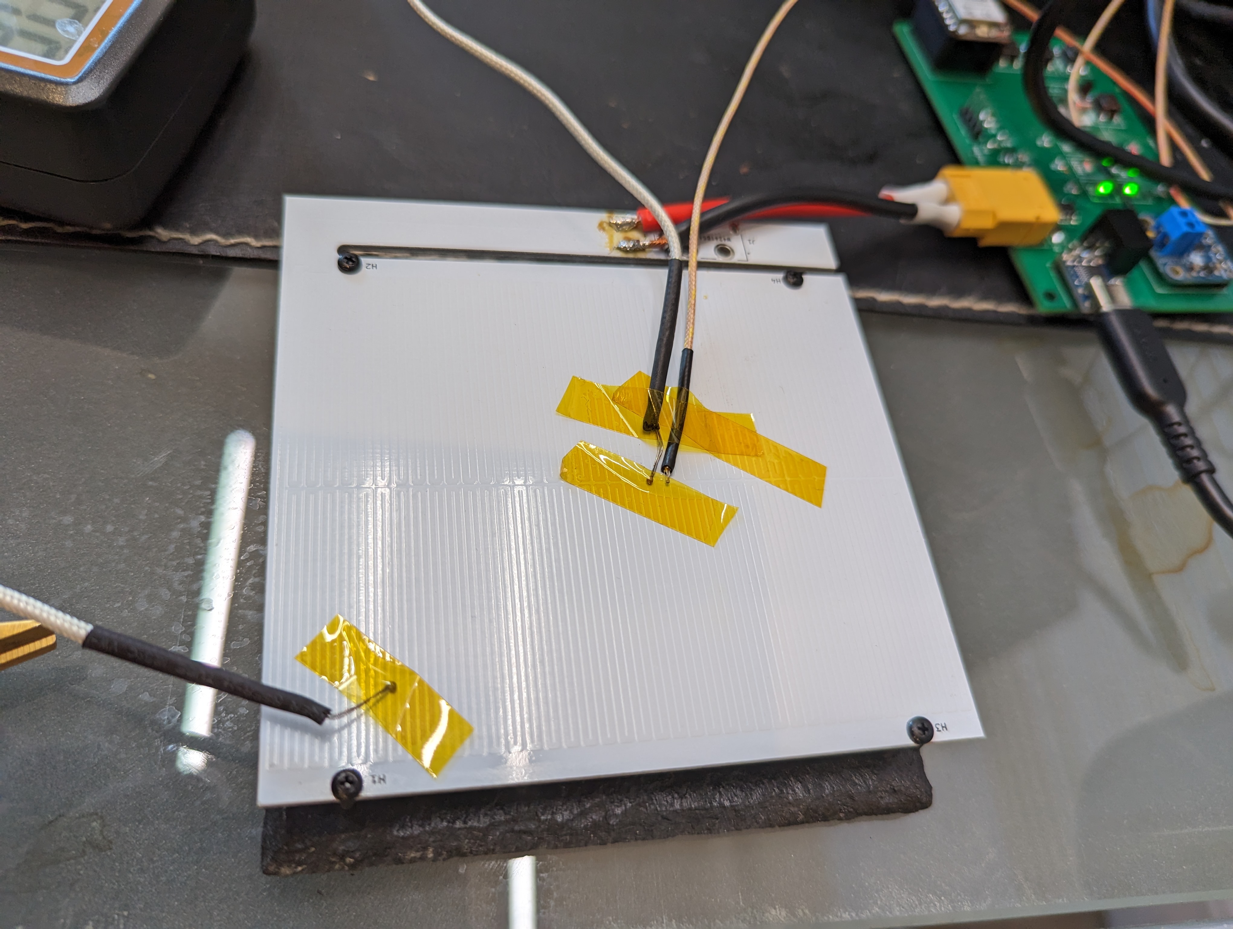
A very basic thermal investigation with two thermocouples showed that the FET was getting hotter than the diode, at least initially. However, I did smoke several diodes in the process.

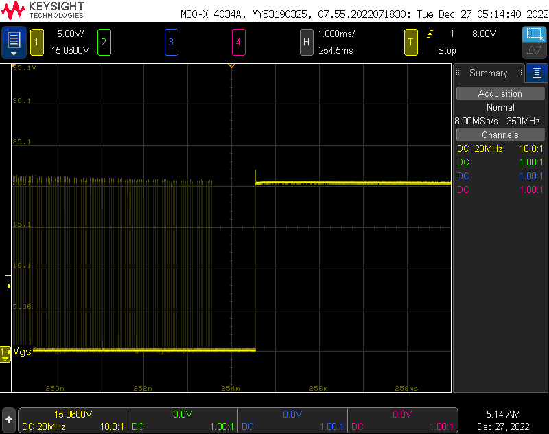
original fet gate voltage. roughly 200 ns of switching time.

Reducing the gate charge did appear to solve the problem, and there was even a note in the datasheet (that I glossed over) about keeping the gate charge below ~30nC. Having a high gate charge is problematic for two reasons- it keeps the FET in a high RDS region for longer during switching, and it requires more power from the gate driver on the LED controller, which also heats up. However, this was not the real problem.

Overheating and Limp Mode:

Note that initially P1, the driver heats up to ~70C. Once the driver gets hot, P2, the diode, gets VERY hot (150C!)

Gate charge was not the entire story. With the FET replaced with a lower gate charge/higher RDSon model, there was still an issue! With the LED aggressively cooled (to allow it to live), the device would still go into some kind of limp mode after a few minutes of operation at high currents (3.6A avg, 12V, about 42W).

This seems to be due to the driver itself overheating, which is due to my poor thermal design. The driver is marked U in the layout above- this is supposed to have a thermal pad connected with vias to ground. I omitted the vias, essentially insulating the chip- no good.

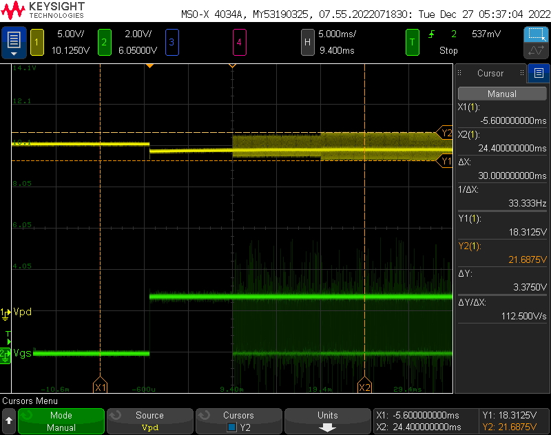
Gate Voltage

Second, at high currents, the regulator needs to switch frequently to keep in regulation. Estimating from the gate voltage above (in terms of time), and assuming maximum 1A gate drive currents, I estimate that the total switching time is at least 100nS with a period of about 1375nS. The average voltage is about 16.5V, so 16.5V*1A*D = ~1.2W. This would probably be easy do dissipate if I hadn’t insulated the chip. Reducing gate charge helped reduce the power this chip was dissipating, but it was not the root cause.

To make things worse, I didn’t add much copper to dissipate heat on the FET, and at least half the copper is on the side of the driver, which actually makes things worse (its easier to for the FET to heat the driver). Adding some vias to a large plane on the back, and increasing the area on the front will increase the area the heat can easily dissipate from.

The reason the diode gets hot is because usually, the diode only free wheels for a short amount of time- when the FET is off. When the driver goes into limp mode, it has to dissipate all the energy stored in the inductor, many times a second.

So the full story is- this driver will self destruct if the driver overheats and goes into hiccup mode. Better thermal design (and eventually cooling it in the ocean) will probably improve the situation, by preventing driver overheating.

A wiser choice of package for the FET might also help dump heat to the PCB, which will be important when this is running in an enclosure. Convection won’t be an option then, and all the heat will need to go into the case.

Efficiency + Thermals:

With the driver sorted, the next thing to do was to smoke test the lamps at high currents. This went reasonably well, with only one LED burning out. As you can see above, the XHP70.3 required a heat sink and passive water cooling in order to prevent burnout. Given that its running at about 42W and only ~25% of the energy is turning into light, this is a 32W heater in a 70x70mm footprint.

This is at about 70C

This is going to be very hard to keep cool, even with the die almost being in contact with the seawater. The good news is at lower settings (around 2A) I should still get a very respectable 3000 lm out of the LED- more than the sola light!

Overall efficiency from power supply to LED was acceptable- in the mid 90’s for lower currents up to about 1400mA, and in the high 80’s above that. while that might seem like poor efficiency, this takes into account relatively long lead wires to and from the pcb, the multimeter, etc, so I actually expect it to improve in the final product, especially once the thermal design is improved.

Conclusion:

This PCB needs to be re-routed with thermal concerns and strapping pins in mind, but overall, it works! This iteration has given me a lot of confidence that the final design will do what I want it to do. I’m also really excited to keep playing with the thermal camera. It gives me a lot more information than the sizzling finger test, and it lets me dig into the context and sequence of the heating.

Sola 2000 Teardown

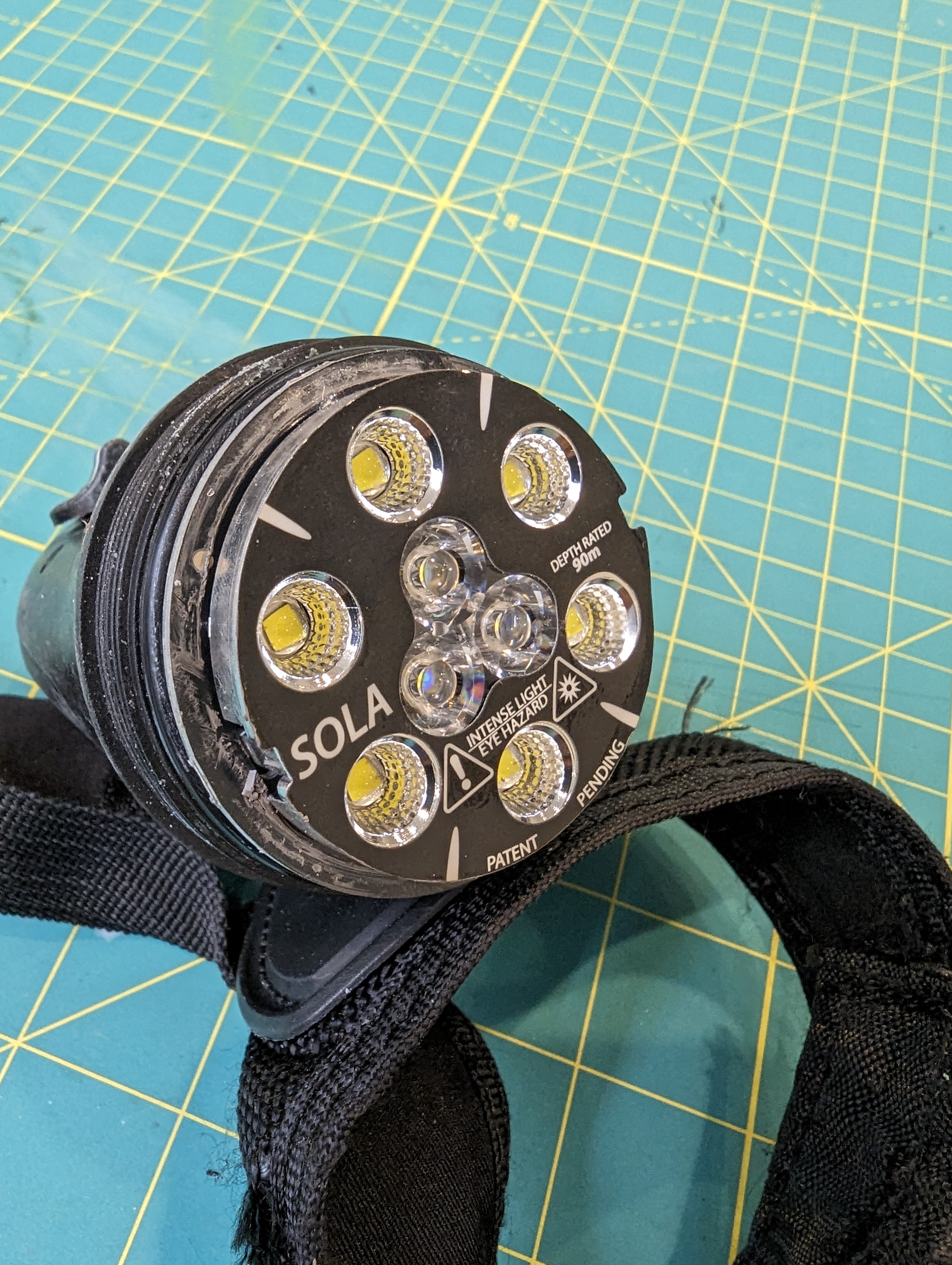
My beloved sola 2000 has finally, after many years of service (and after buying it secondhand) flooded. High power LED drivers and seawater do not mix well, and this light is at its EOL.
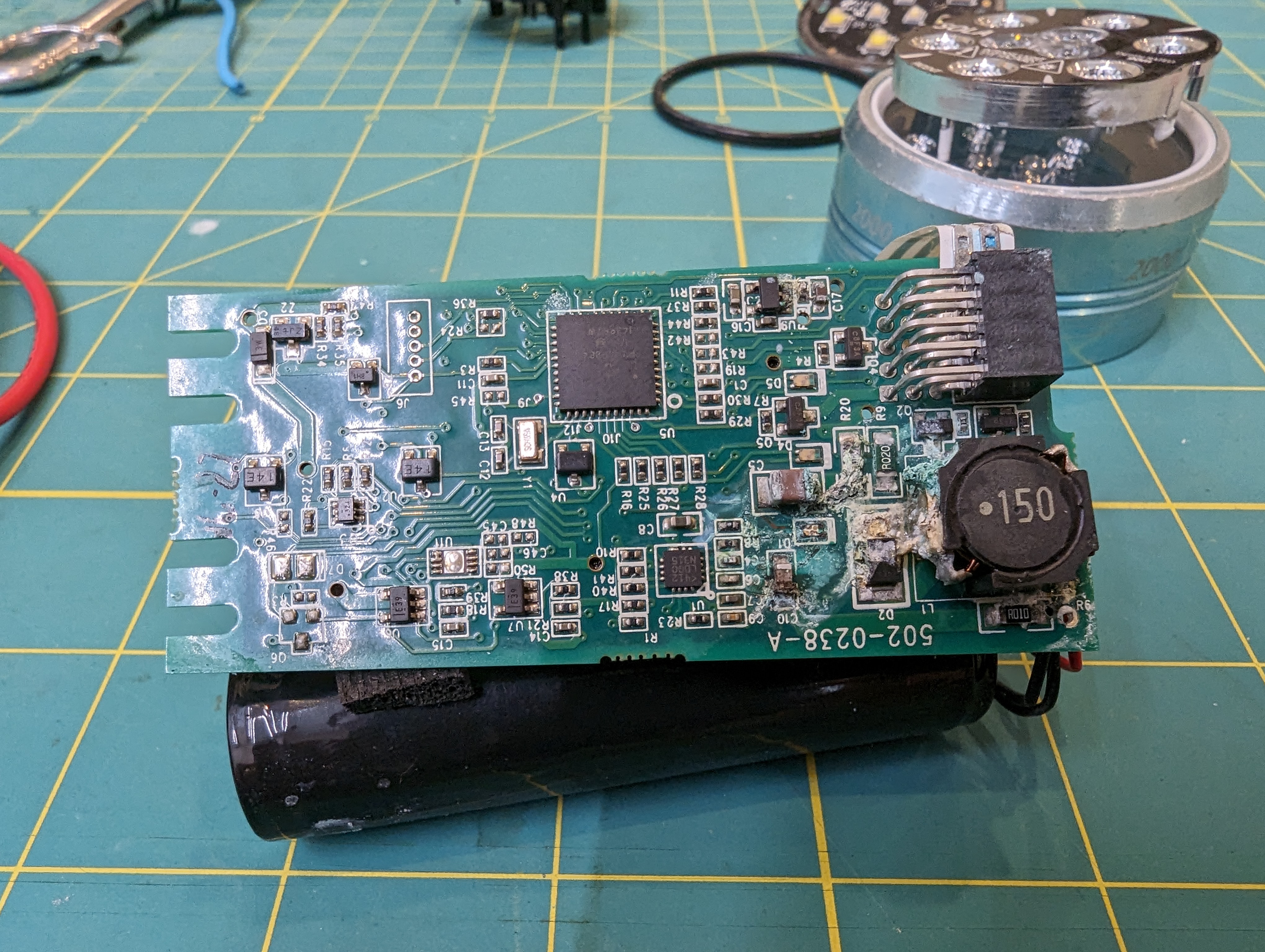
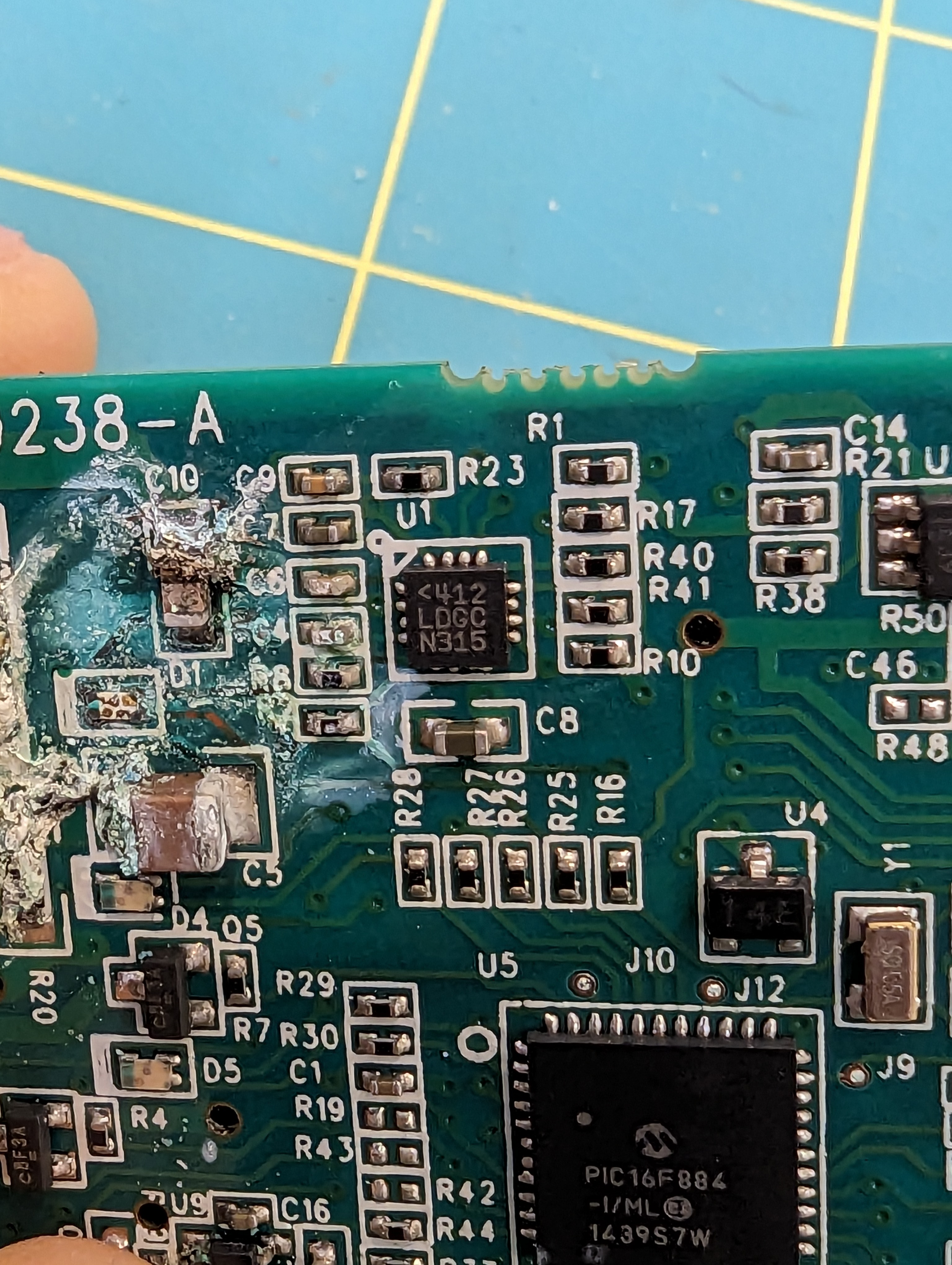
visible corrosion damage to the PCB

I have always wondered what was in this wonderful light, and now that its toast I don’t have any issues tearing it down to find out! There are a lot of very clever design decisions in this light, and a lot to learn.

Light head
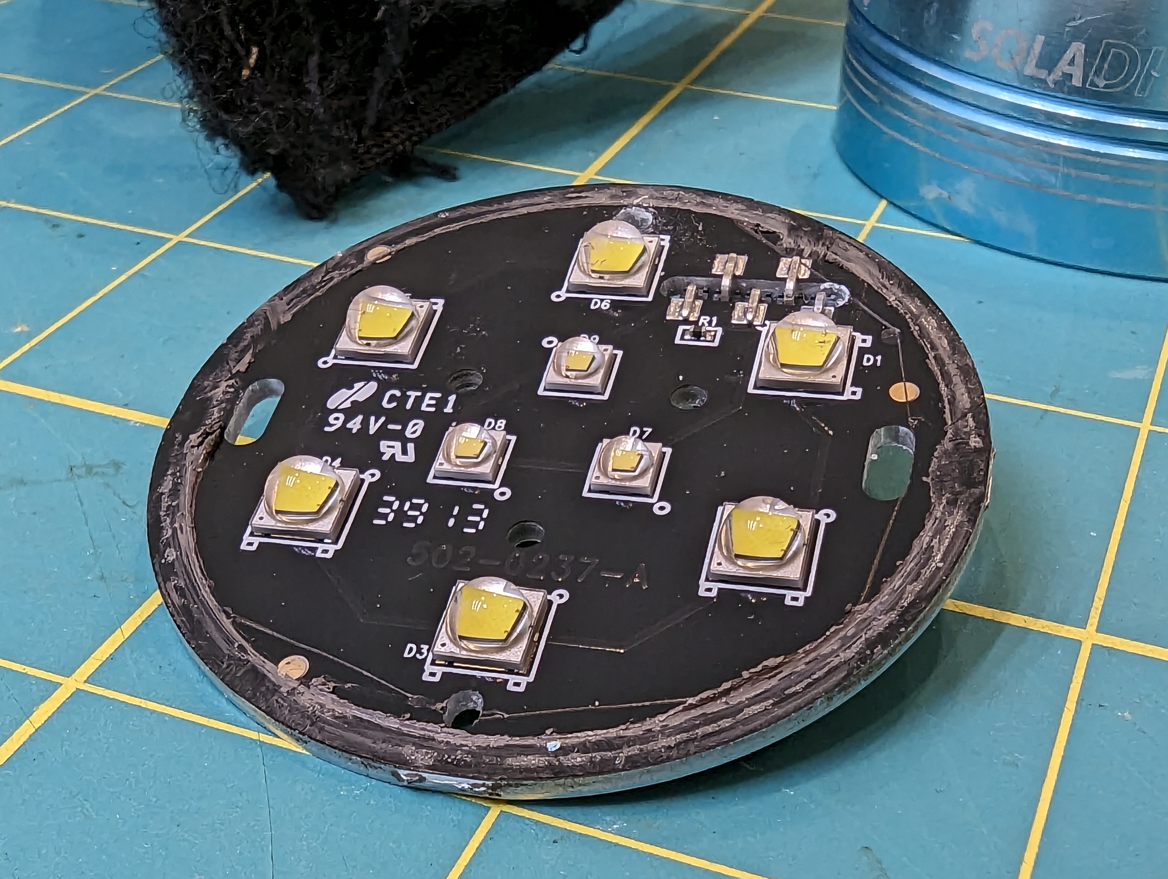
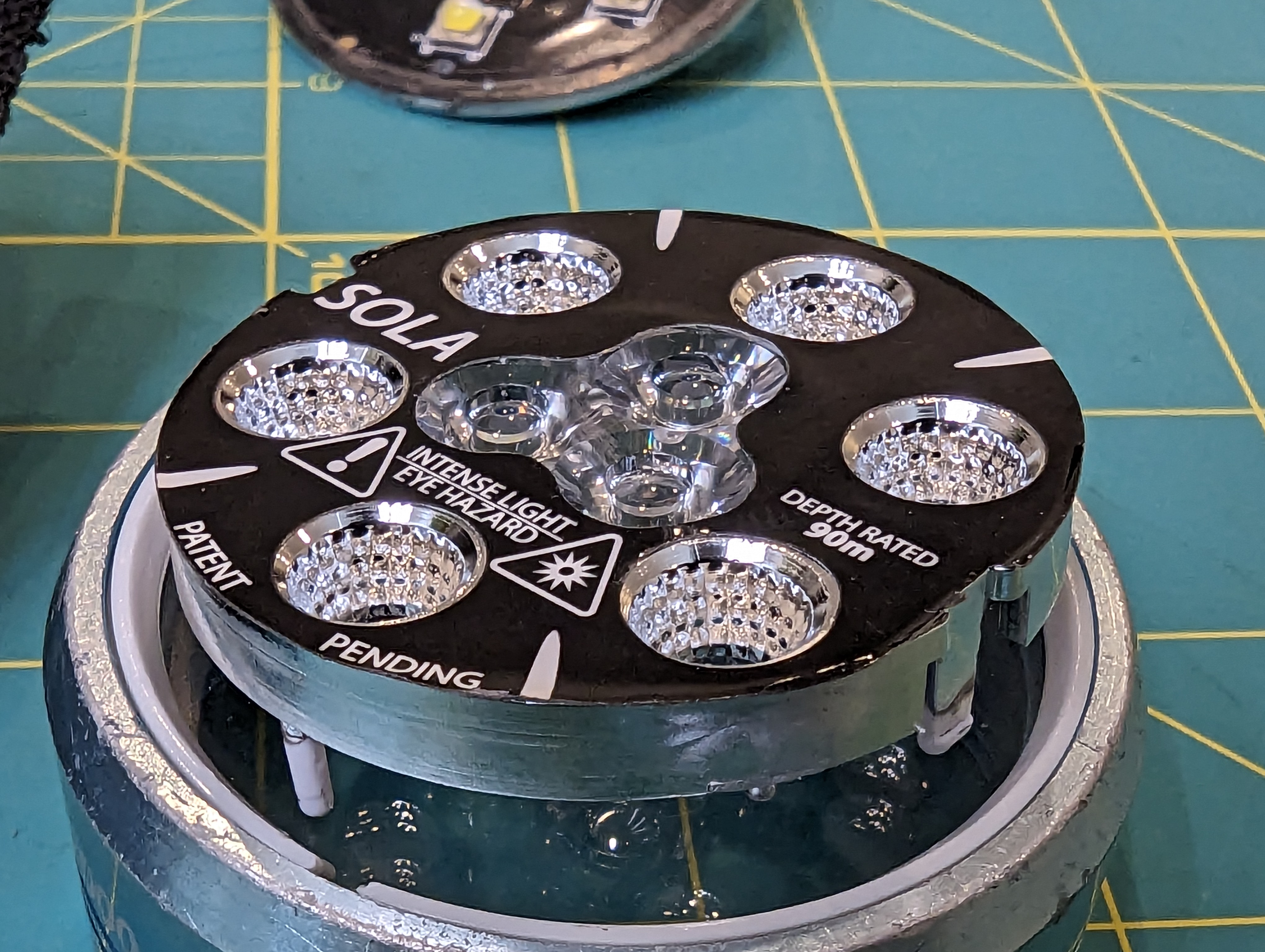
The light head has two rings of LEDS- one for spot lighting and one for flood lighting. the small inner ring of three LEDs is the spot light, and the outer LEDS are the flood light. Given the package size and general shape the LEDS, I assume the inner ones are CREE XP-E2 LEDS, and the outer ones look like CREE XM-L2 LEDs.
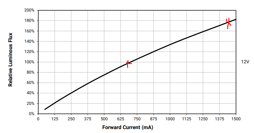
from XHP50.3 datasheet- note that 2x current does not reach 2x luminous flux. additionally, 2x current increases Vf, which makes it even less efficient than expected from this plot

Having multiple LEDs is very smart, because LEDs run more efficiently (in terms of light per heat) at lower currents. It also spreads out the heat loading of the PFB- CREE says to estimate 75% of LED power to turn into heat instead of light- that means that a 4W LED needs to dissipate 3W of heat.

Given the stated lumen output of the light, I would guess the flood lighting runs around 9-10W, or 1A at about 9V. The ring of 6 flood LEDs probably run at about the same current (1A) but at about 18V, for an output of 18W. This means that about 7-14W needs to be dissipated. This seems to be done through good contact of the aluminum PCB with the metal ring that goes on the front of the light. If you look at the PCB photo above, you will see a smear of thermal grease along the edge.

Running multiple LEDS efficiently means spreading the heat around, especially for the radial LEDs, which are closer to the heat-sinking bezel. Its also important because the light is powered by a relatively small battery pack.

To prevent overheating, it seems like there is a single thermistor on the PCB as well. This will let the controller throttle the output when the emitters get hot.

Optics
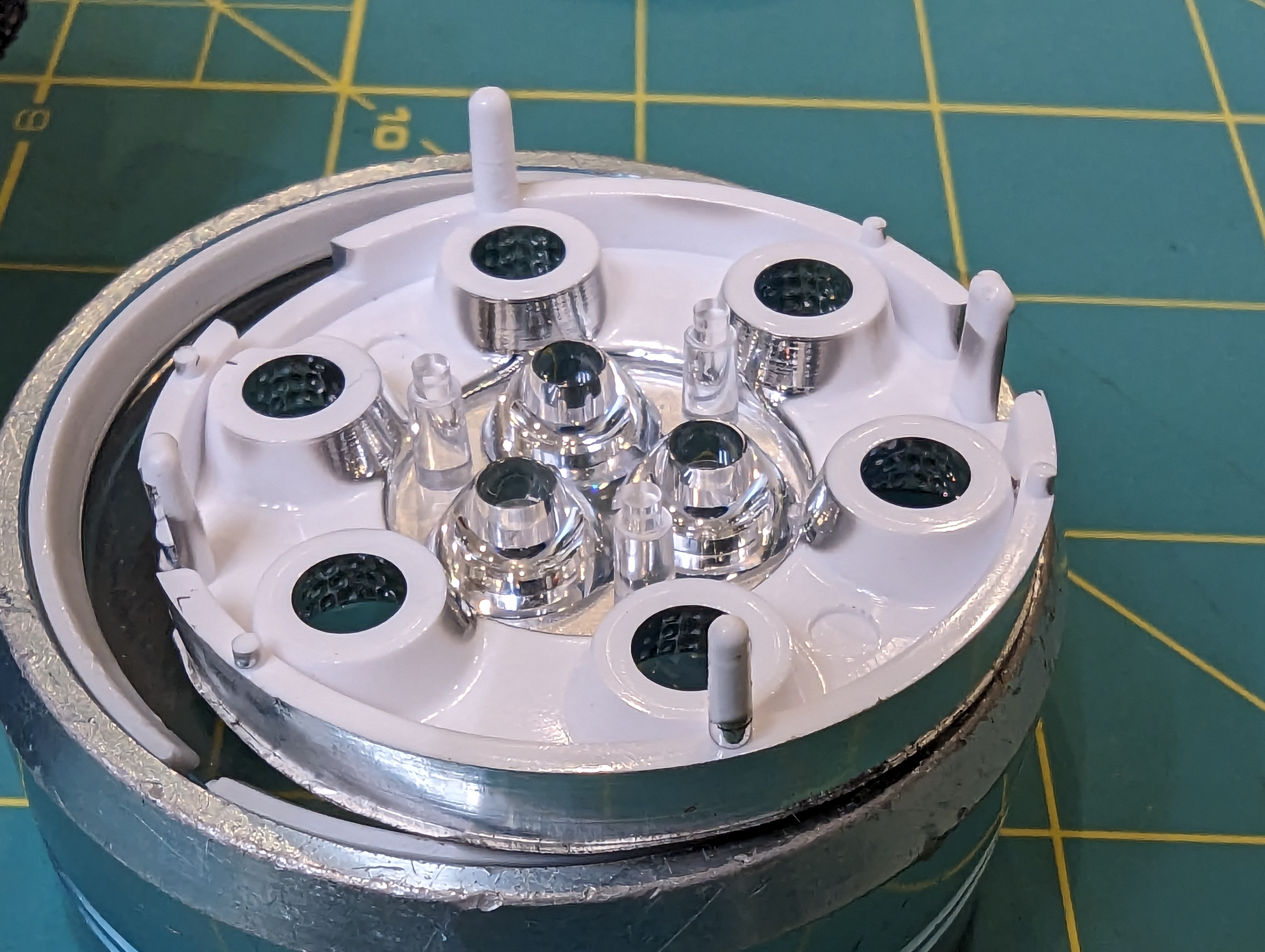
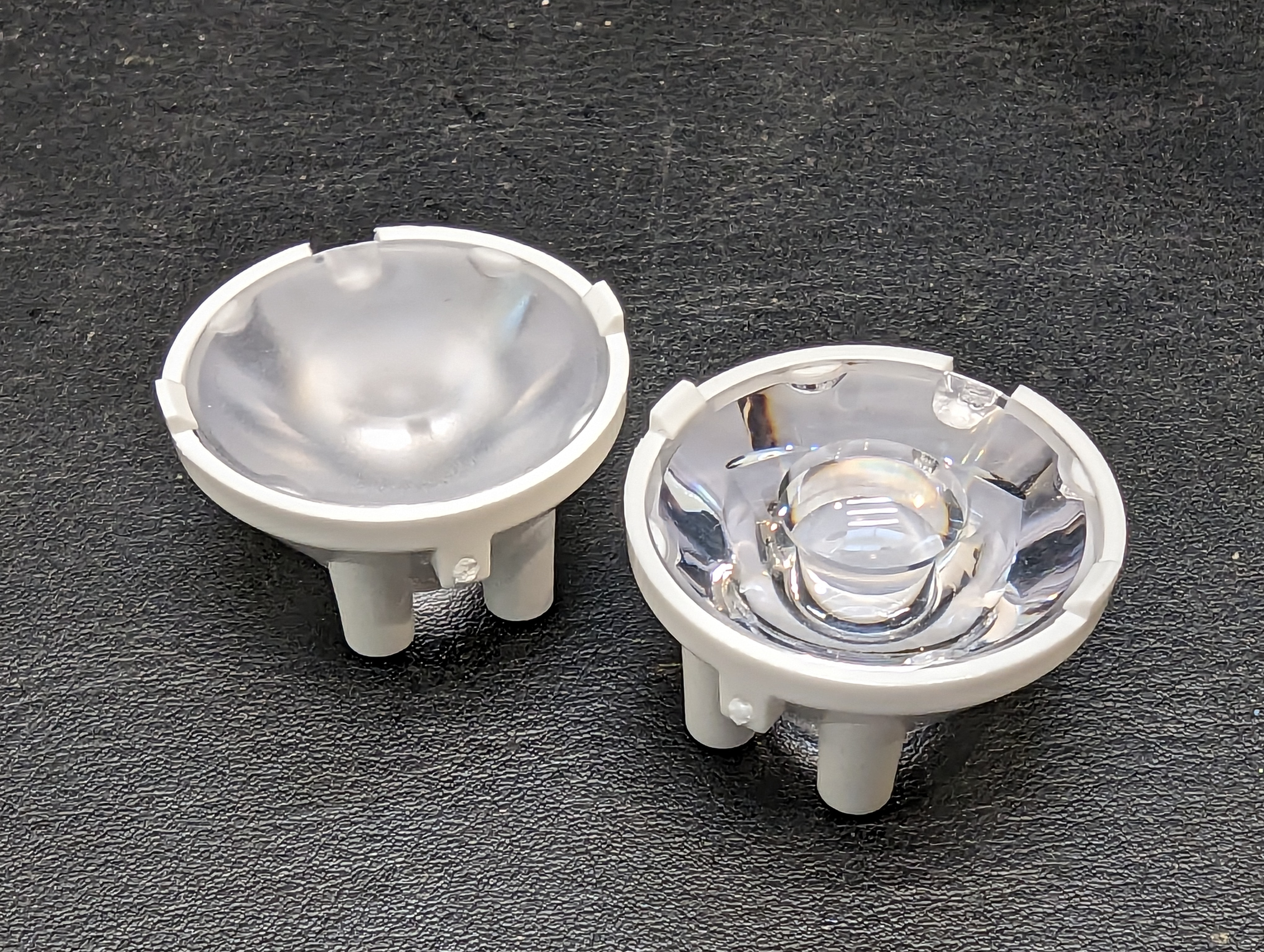
The optics look a lot like they are made by carclo (wild conjecture). There are two styles- reflectors for the spot lights, and a total-internal reflection style optic for the spot light. I do wonder if there is any attempt to collimate the spot beam to make it extra tight, by biasing the three spot beams inwards.

LED driver
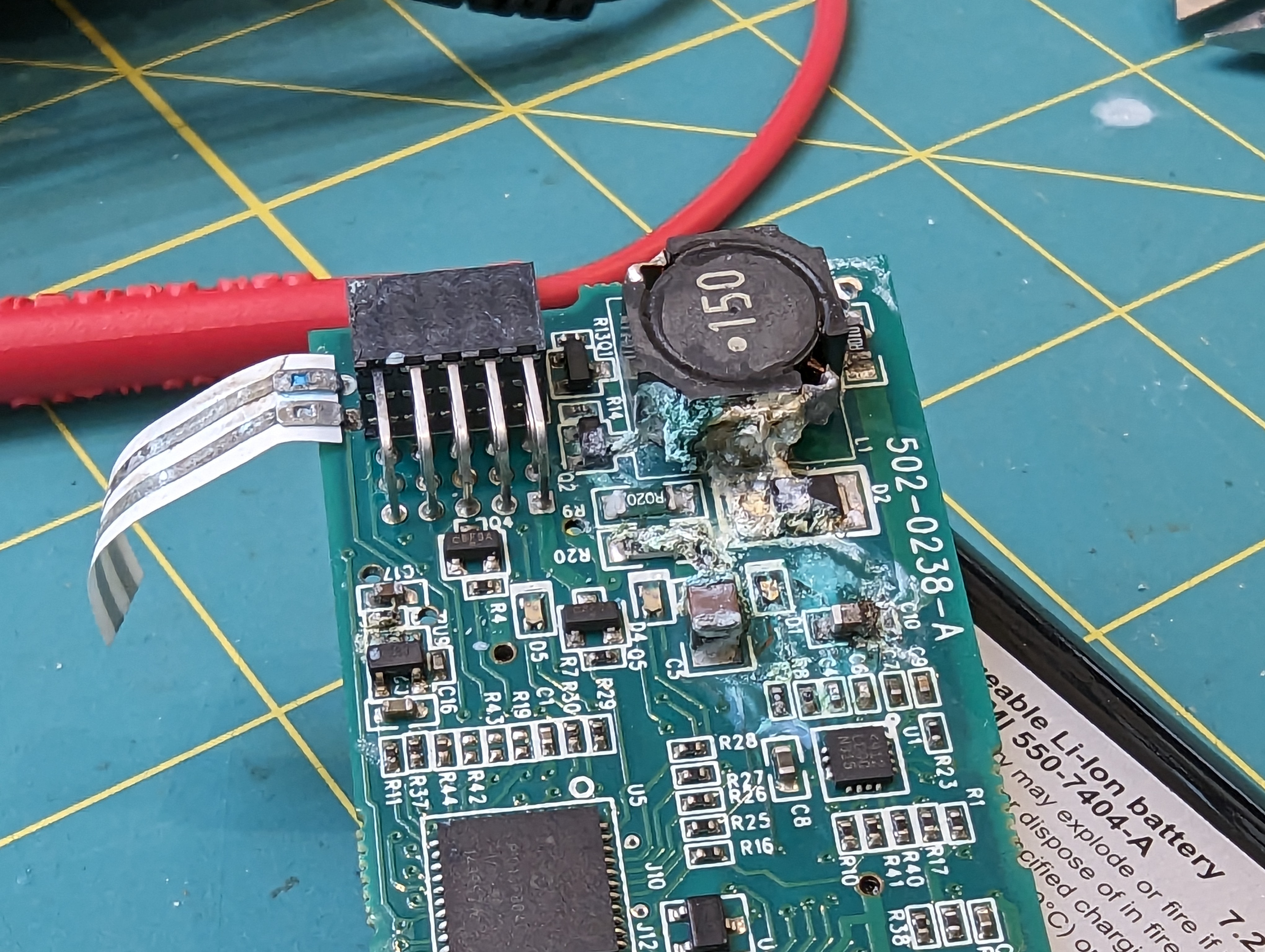
The LEDs are driven by an LT3755 wide-input rage LED driver. This driver is probably operating in boost mode all the time, since the battery voltage is too low to drive any of the LEDs. Interestingly, there is only one driver (just like in my design) but there appear to be two current sense resistors. I suspect these resistors are switched in for the spot and flood modes (on the high side, with a PFET), and then the overall brightness is controlled by PWM. This makes sense because these LEDS are probably operating at reasonable efficiency, so there is no advantage to turning down the average operating current.

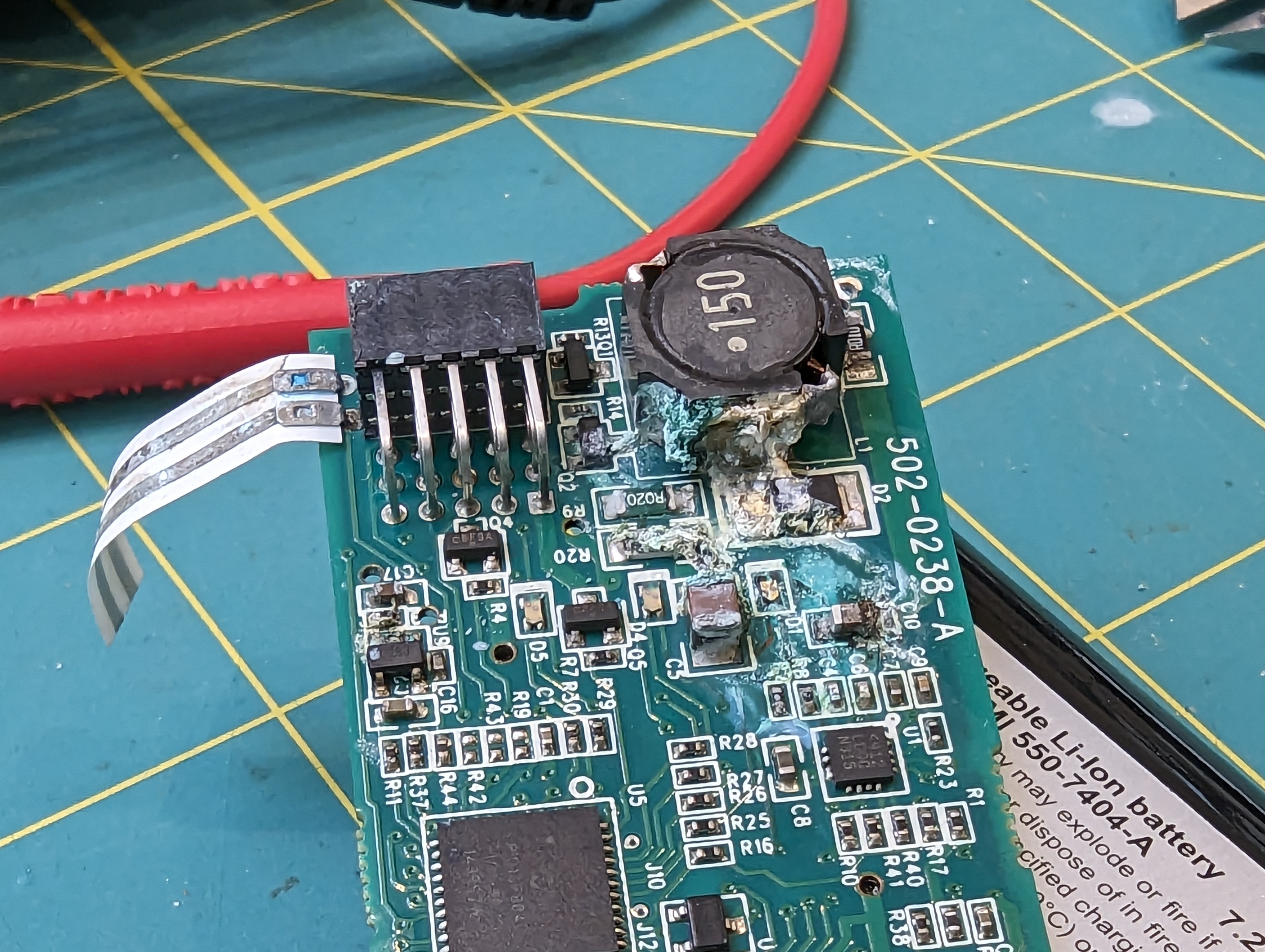
As you can see, most of the corrosion/damage happened near the boost converter. It is close to where water can come in, and it is also where the highest voltages exist on the board. Seawater can cause a short between the current driver outputs, which would then tend to increase the output voltage until the current set point was reached, or until the driver maxes out or reaches some thermal limit- in other words, its a vulnerable circuit.

Flood sensor?
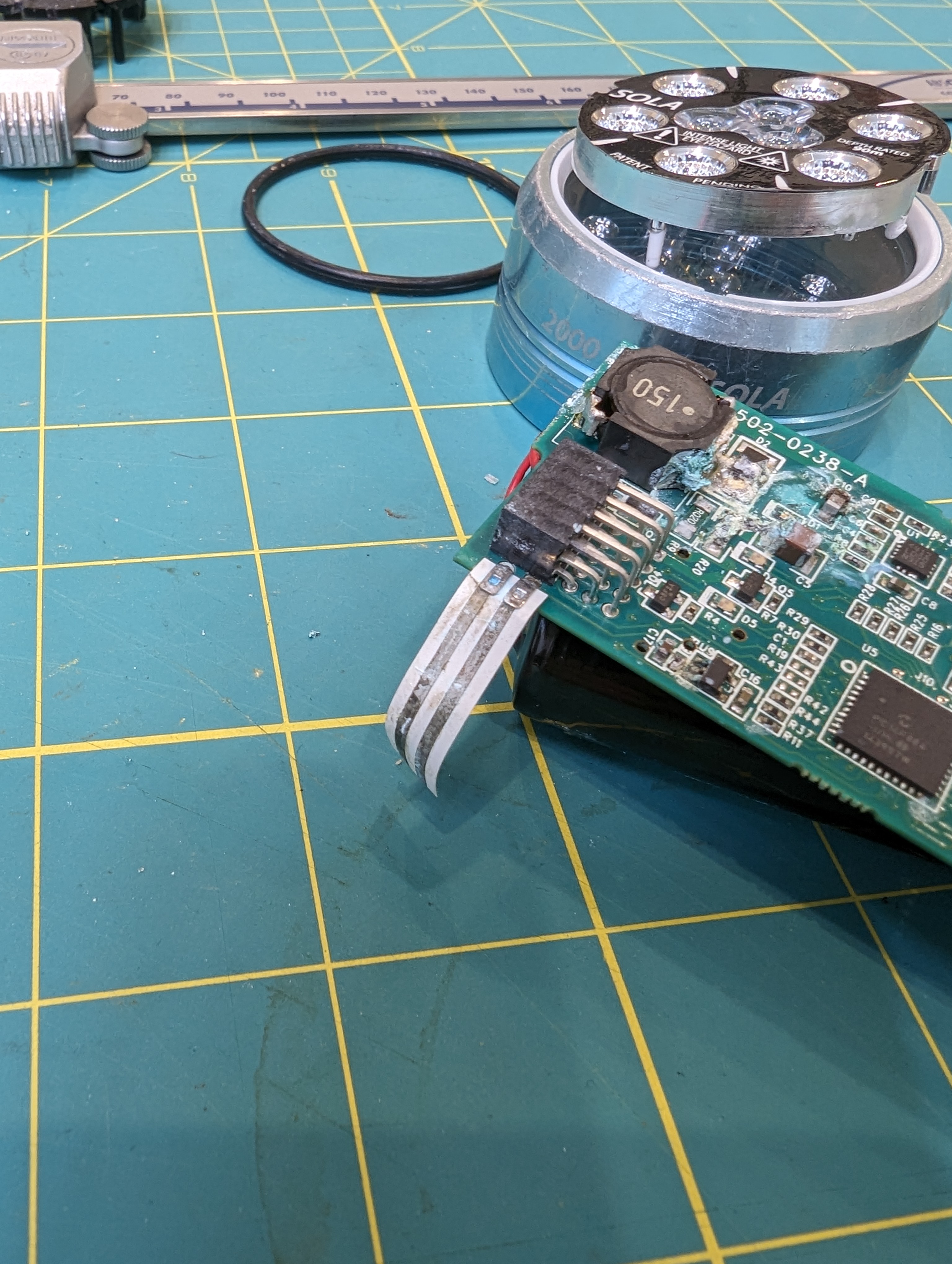
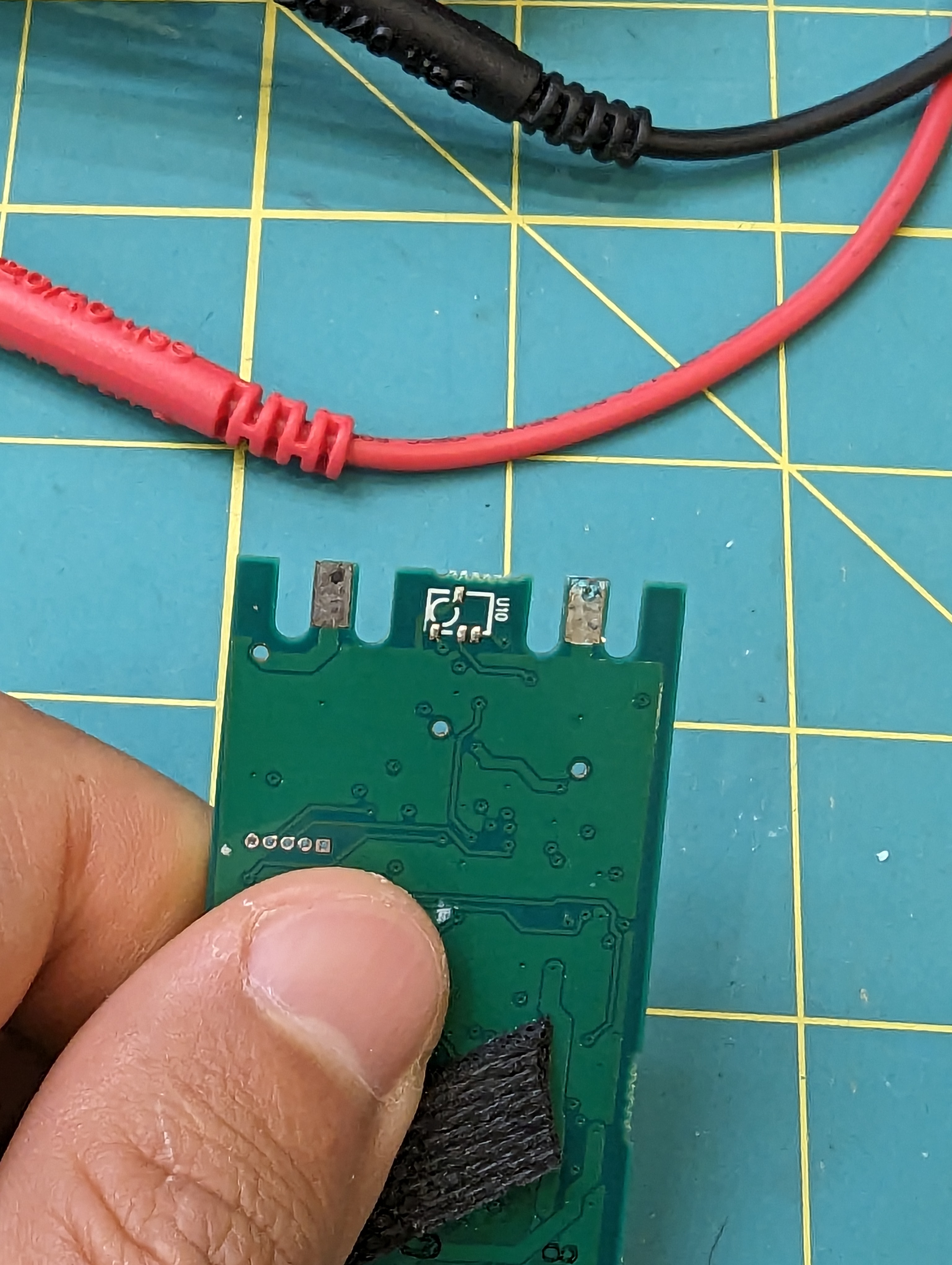
This board has something pretty unusual on it- a big floppy ribbon with conductors on one side. At first, I thought it might be some kind of temperature sensor, but I think it is a flood detection circuit- if it gets wet, it will alert the micro to shut down the led driver. This makes a lot of sense, both to protect the battery and the PCB. If the lamp is dried out after being protected from a flood, I imagine it would be just fine.

Magnetics + Micro
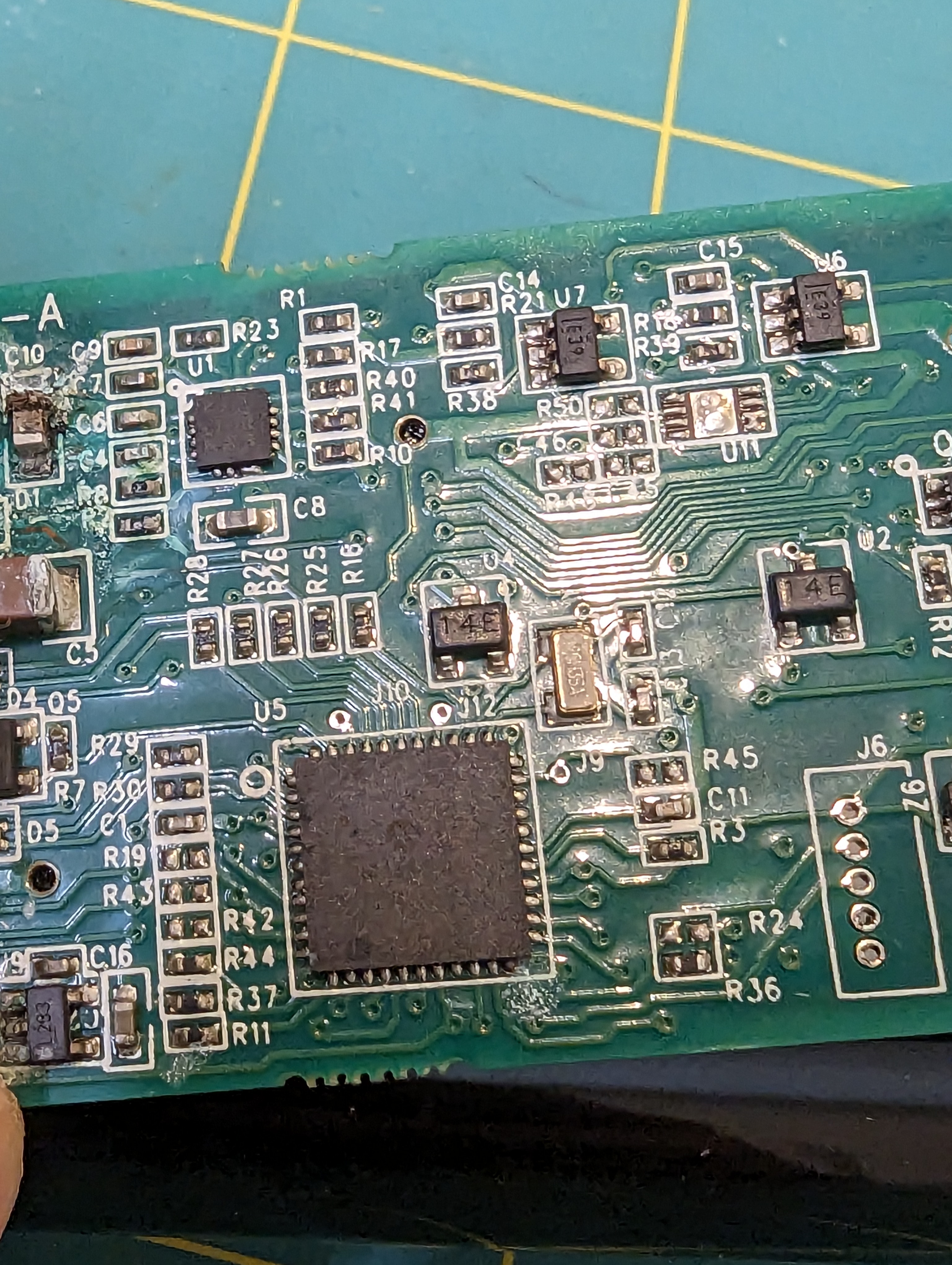
The micro is a pretty basic PIC16F884. The interface is much cooler. There are three evenly spaced IC’s marked “14E” on the PCB. I am guessing these are made (or were made) by NVE, since a lot of their ultra-low-power magnetic switches have that as a portion of the part number. This allows for control of the light without having an extra hole (leak point) in the case.

Power connections
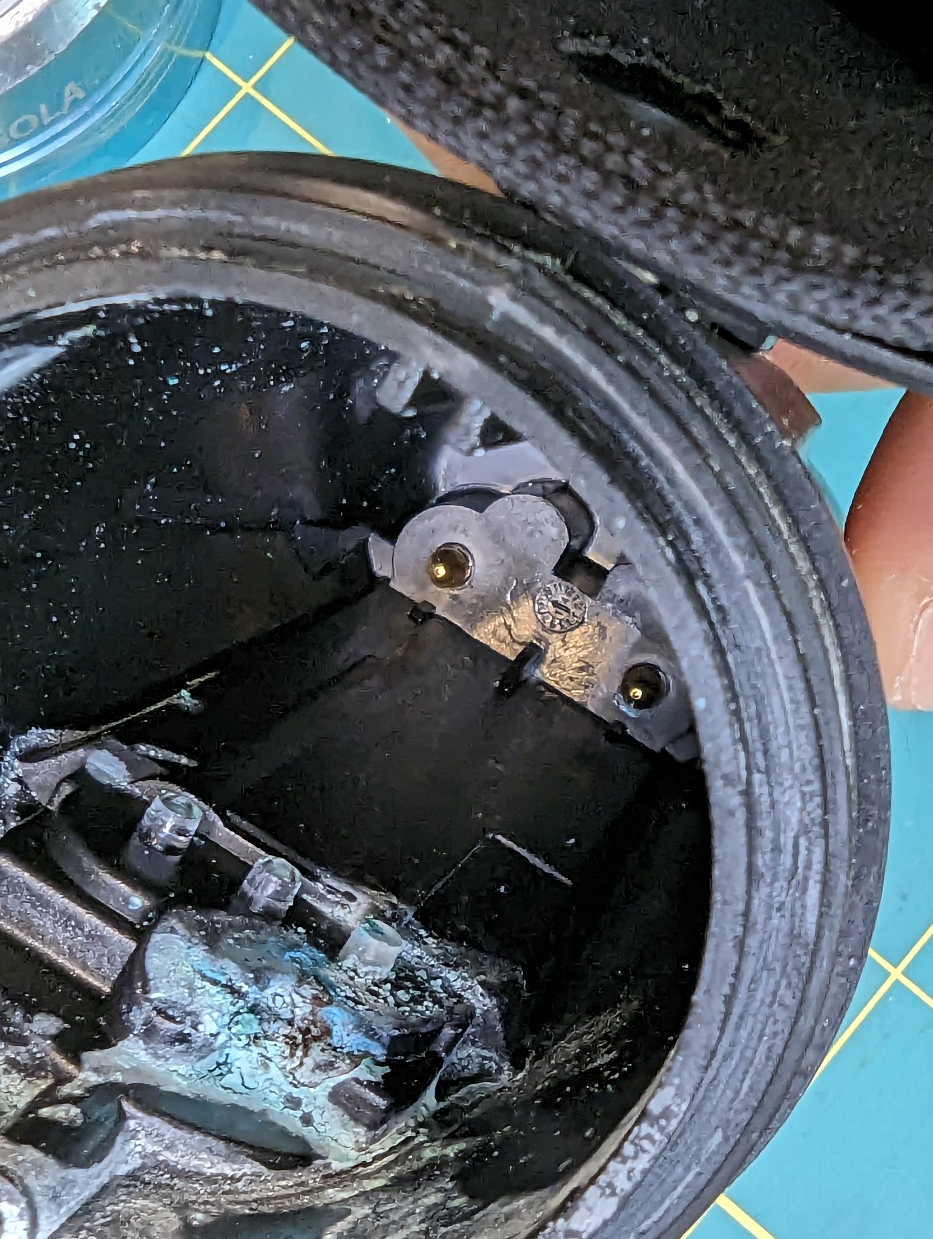
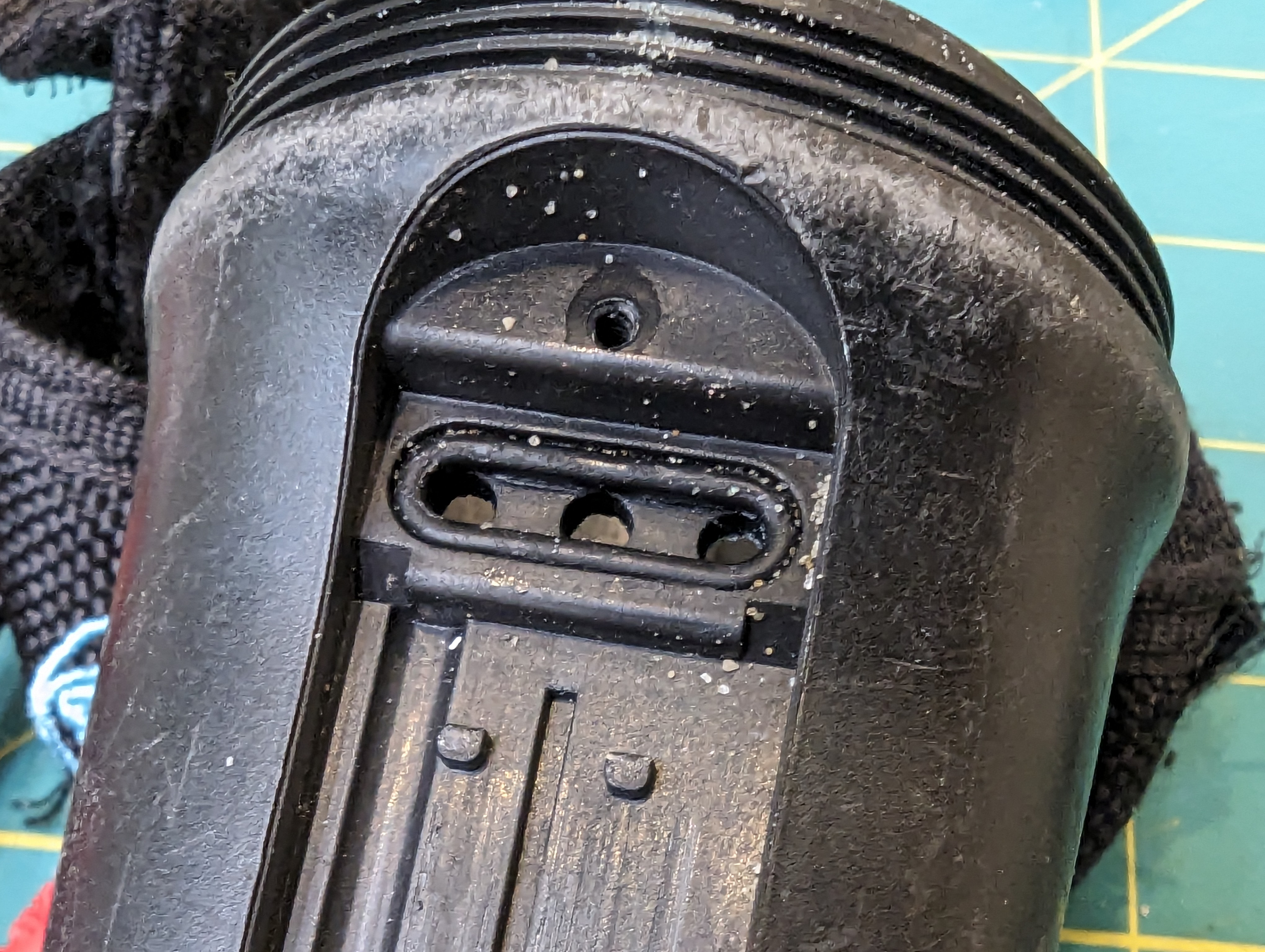
Surprisingly, the power connections are made by wedging the pcb onto the gold contacts in the back of the case. Never in a million years would I have though that this would work so well, but some clever ribs in the back of the housing push the skinny pcb cutouts/contacts onto the gold plated pins.

Autopsy
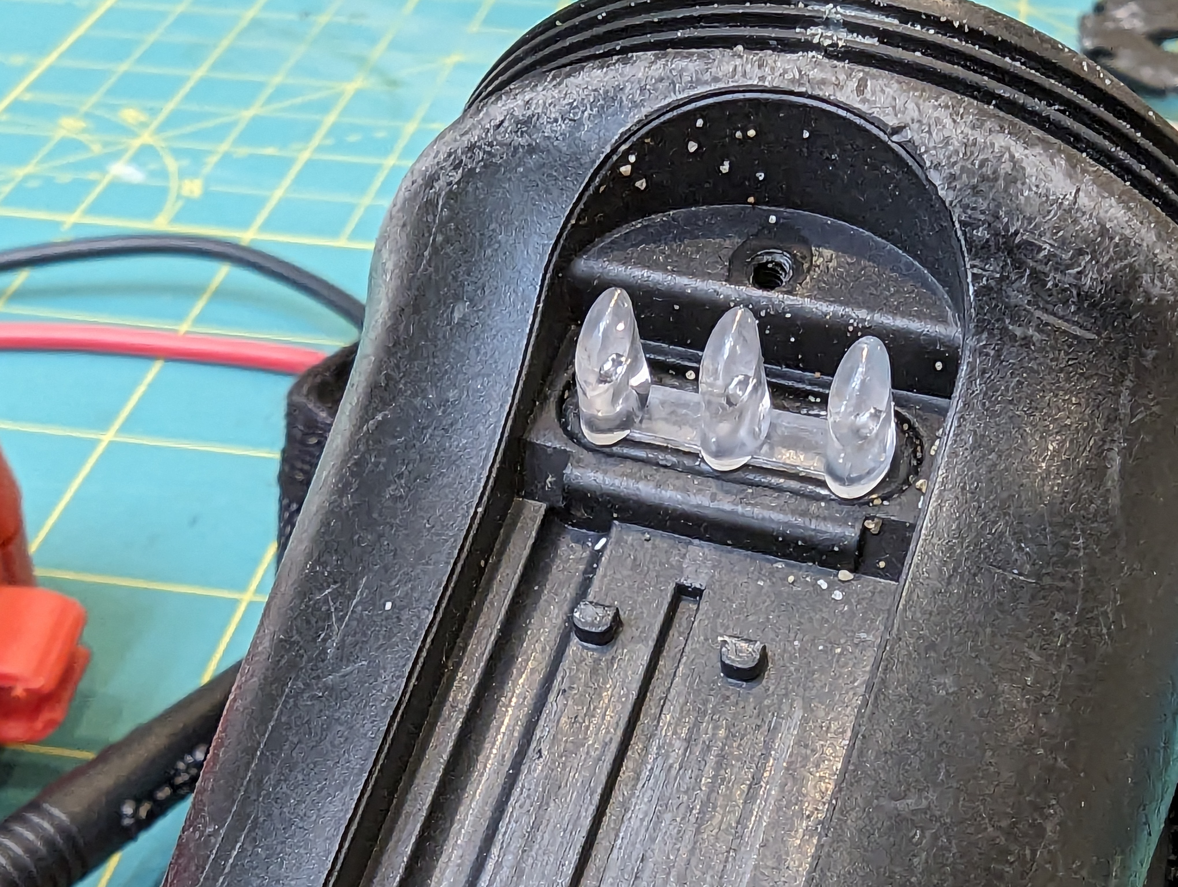
I’ve always liked the sola lights because they are “factory sealed” and there are no waterproofing components that need changing regularly. Inspection of the front oring didn’t yield any interesting results, but looking at the light pipe seal, I have some suspicions that this might be where the light failed.

The corrosion is right under this seal, although that is also the most likely place for corrosion to happen, so its not a slam dunk. However, this is a circumferential static seal, and there are things I dont like about it.

Specifically, the surface finish of the light pipe is not very smooth on the contact area of the oring (difficult to photograph), and the whole light pipe can rock gently (although this is somewhat prevented by the bezel). The bend radius of the oring is also pretty tight compared to the diameter. The radius is about 2x the diameter, where the best practice would be about 6x the diameter.

Obviously this is a fine design, given that this light has lasted many many years. That said, I am suspicious of this seal.

Closing thoughts:
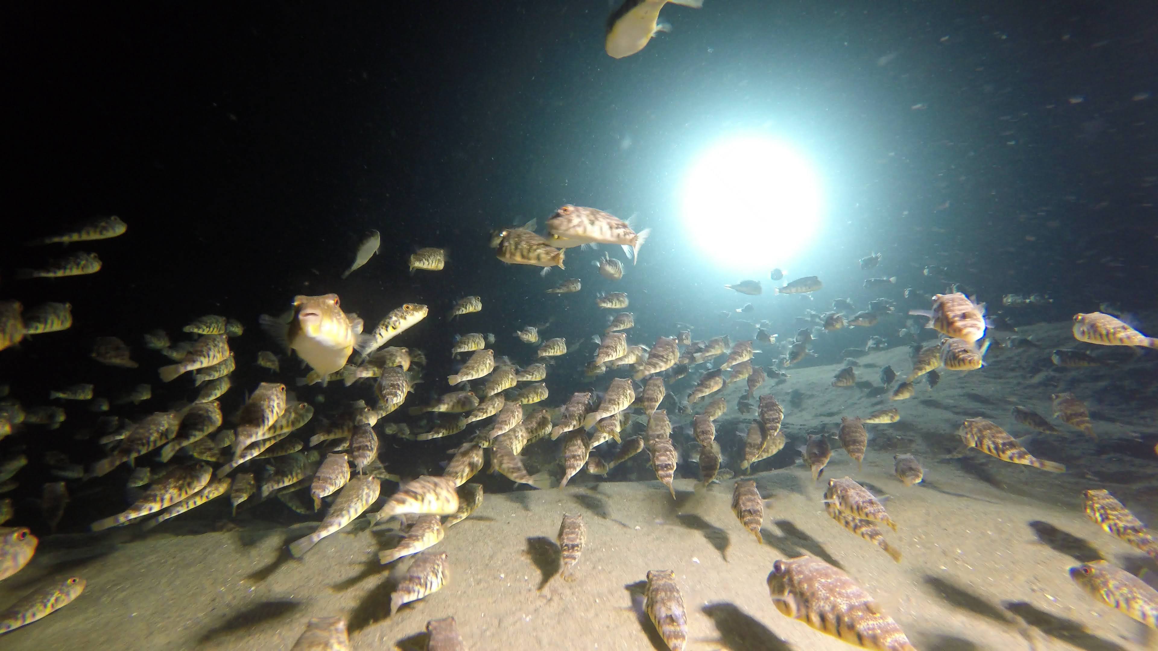
puffer-palooza at folly cove, illuminated by this light…

This light is pretty tidy from an engineering prospective, and it was a great dive light. I am still curious about what is shared between different models- how is it different than the sola 1500? from the spot lights (the driver here could easily drive a COB)? How did they reuse parts between the designs? And what on earth is that funny three-tier connector for (different models?).

I won’t be getting the answers to these questions but its fun to see what made this thing tick for so long.
DIY Canister Dive Light – Design

I recently found out my sola 2000 torch is torched- water got in and corroded the connectors. while it might be technically salvageable, I used this as an excuse to start another project- a canister dive light. I love my sola light, but the battery does not quite last two dives, especially at full blast. This means I need to bring two lights, two chargers, and two lights, and that is a little inconvenient. It also means I spend a lot of time futzing around underwater going from low to high power mode. This is surprisingly annoying, especially since I have to use two hands to switch modes.

Armed with google, hubris, and kicad I set out to design my own dive light.

Design Goals:

The goal is to build a dive light, with spot and flood modes, just like the sola lights. I want a burn time of at least 3 hours at a reasonable brightness- this is well over two recreational dives. I want it to be a canister light so I can run it full blast for the whole dive, temperature permitting. And I want it to be about as bright as the sola lights. And small. And I want a pony to go with it (kidding).

Optics and LED choices

There are a lot of constraints on this project, starting with thermal and optical considerations. There are only so many off the shelf optics, and without much in the way of a mechanical prototyping department, I want to minimize iterations. The simplest way to do this was with single LEDs and off the shelf optics. Carclo has not only an impressive array of parts to buy, but they also have charts/images to go with the optics with different base LEDs.

The problem with single LEDS is that the efficiency of the LED suffers at high outputs. This creates a lot of heat. Hopefully I can use the ocean as a heatsink. CREE seems to make hands-down the best high output LEDS, and after some careful considerations of what is available in low quantities, I decided on one XP50.3 and one XP70.3 LED. Two XP70.3’s would be better, but the beam pattern on the spot light would be too wide, since I can only get the XP70.3 with a dome lens.

Driver

Next up was the driver. It seems pretty useless to have spot and flood lighting on at the same time, and as you can see, the PCB does not have a lot of room on it for another big driver and inductor. Instead, I intend to share the high-side LED driver across both LEDs by low-side switching them. The header on top is for programming, and as a breakout for interesting pins.

Microcontroller Selection

I begrudgingly picked the ESP32 as my microcontroller. It seems like a shame to have and not use a ton of the peripherals on there, but its cheap (compared to an attiny), small (but still has a lot of pins), and in stock (unlike the atsamd series). This requires a 3v3 regulator, and due to size and laziness constraints I opted for an integrated DC-DC module. These are awesome, cheap, and easy to assemble, which is nice because I already had a lot of 0402 parts.

Emitter (LED) Board

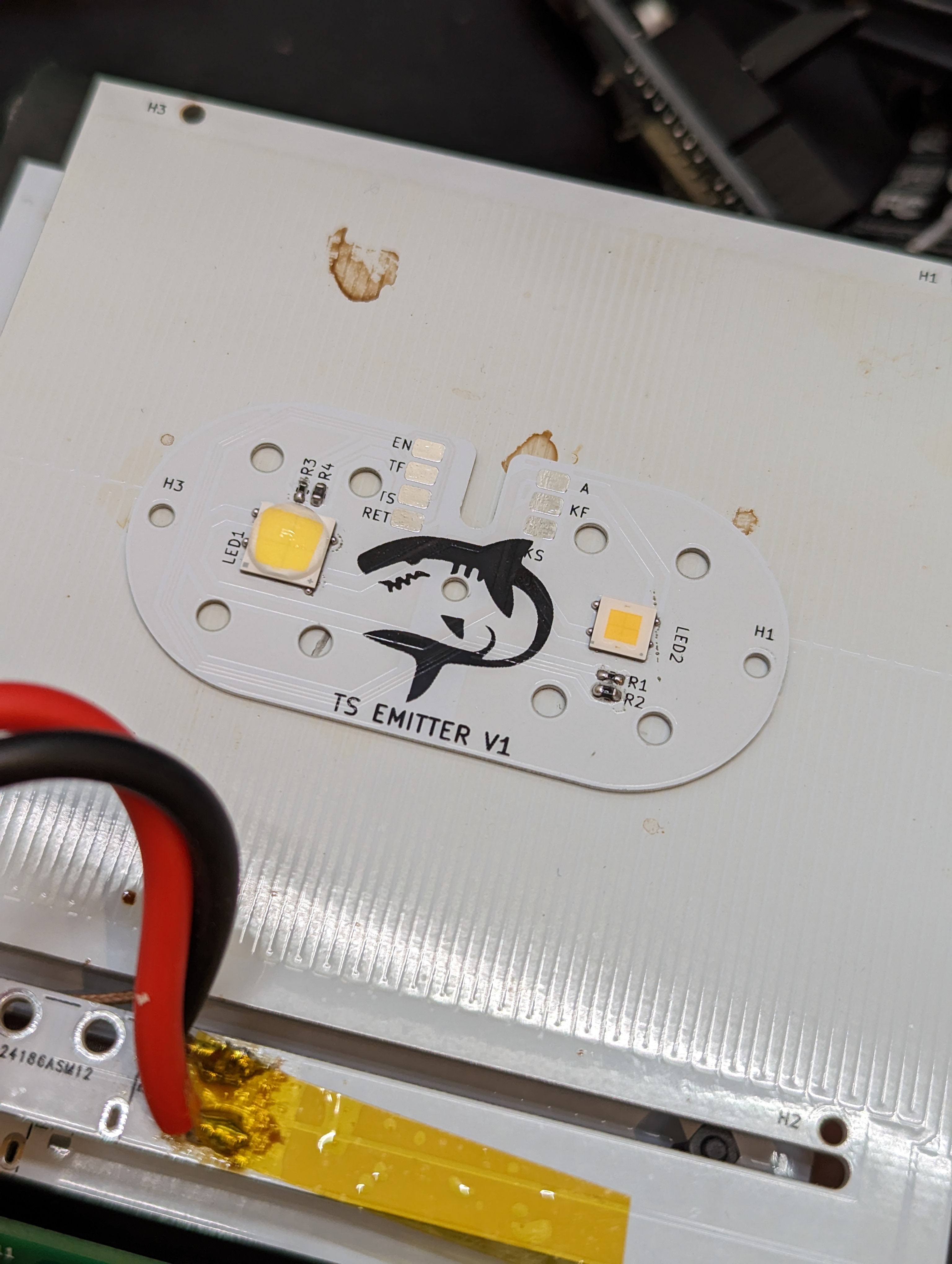
The emitter board is aluminum, for better heat conductivity. At full blast, this will need to dissipate ~30W! In addition to LEDS, there are a couple thermistors for temperature measurements, placed near the LEDs. Given that each LED is a multi-watt heater that could probably melt itself off the board (with low temp solder), it seems prudent to monitor temperatures.

next up: firing up the retina blaster!

Junk Bin Spincoater

With the tachometer done, the next step was to get the ancient BLDC and ESC wired up and figure out how fast they were spinning. I know that the motor spins very fast but I really didn’t know how fast it was. It turns out that the speed is mostly too fast.

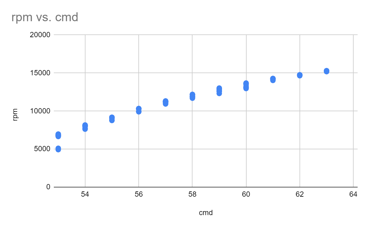
Here I plotted the RPM vs input command, which is basically in “hobby servo degrees” since that is how the ESC expects to get commands- a pulse every 20ms where the width of the pulse corresponds to…something. I mostly care about speeds between 5-10k, which gives me about 4 settings. I suspect that by decreasing the voltage of the power supply, I could decrease the minimum speed by limiting the free-run voltage across the motor.

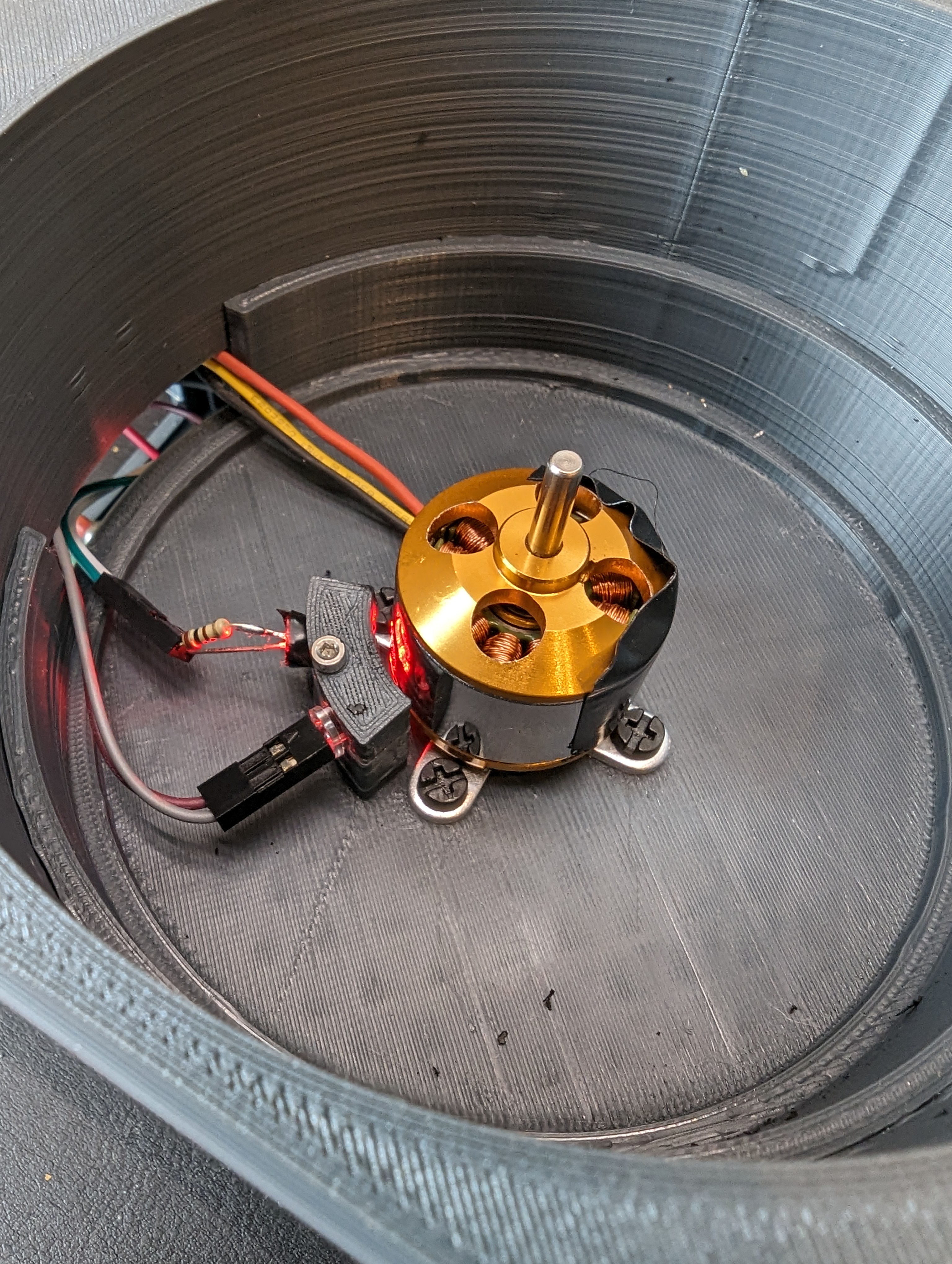
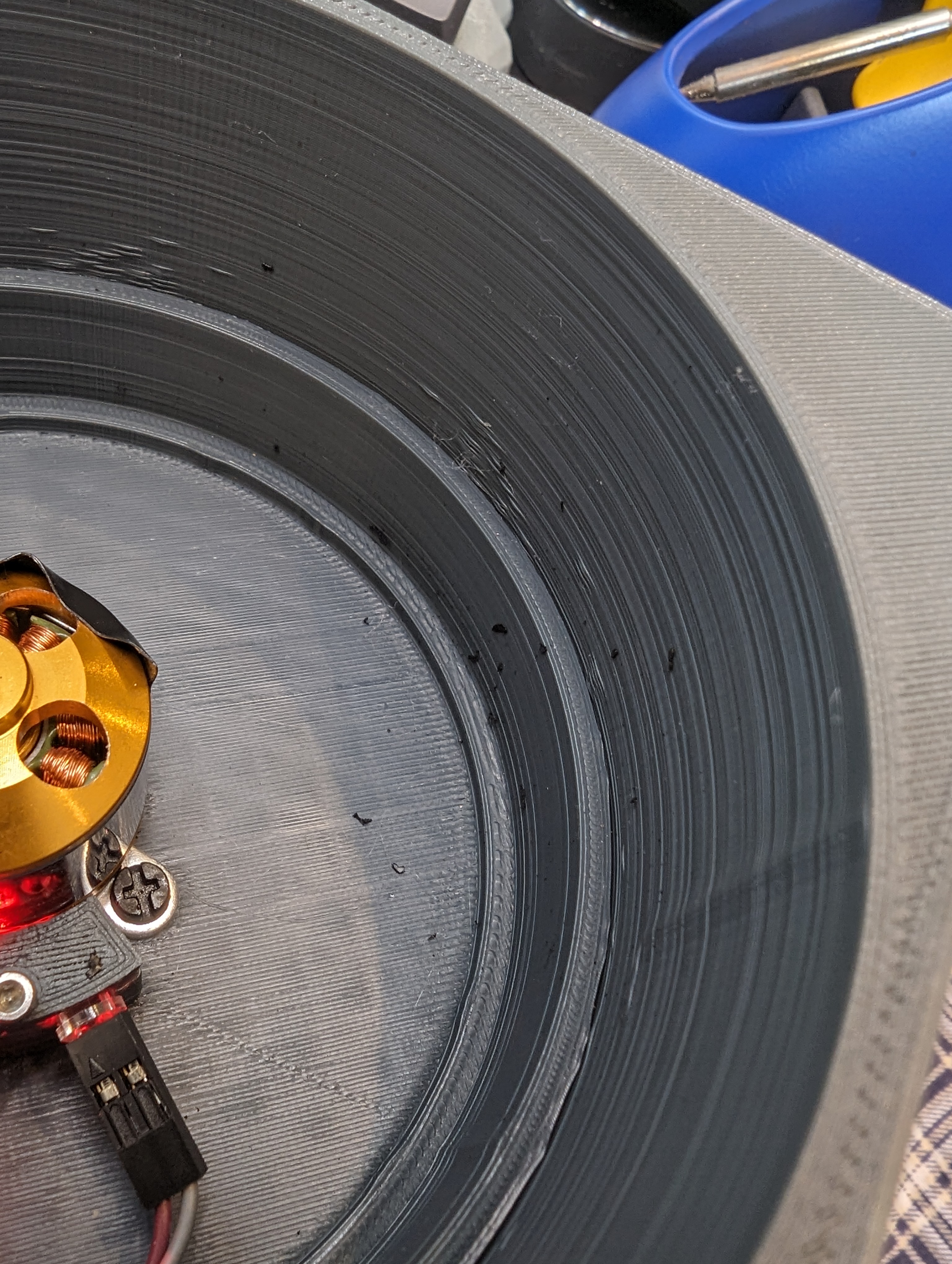
As I said, its not clear exactly what the mapping is from pulses to rpm, since I don’t really know how the controller works- is it closed loop? is speed control achieved with voltage limiting, or is there actually feedback? Right now it doesn’t matter since my goal is just to make things spin fast. As you can see here, the motor spun fast enough that the tape I was using as part of the encoder ripped itself off and disintegrated all over the inside of the container.

Next Up: A PCB

absolute chaos

Based on a lot of really annoying fiddling and having parts get de-soldered during assembly, I have decided I really need a PCB for this project to prevent it from self-destructing by vibrating my deadbug soldering apart. A display, and maybe some buttons would help make it fully usable.

Junk Bin Tachometer

I ended up with a day to work on my spin coater in between a few other projects. Originally, I wanted to make a nice spin coater but because I am basing the design on a random ESC and motor that I bought 5 years ago, I decided the rest of the build would come from the junk bin as well- at least that would be fast.

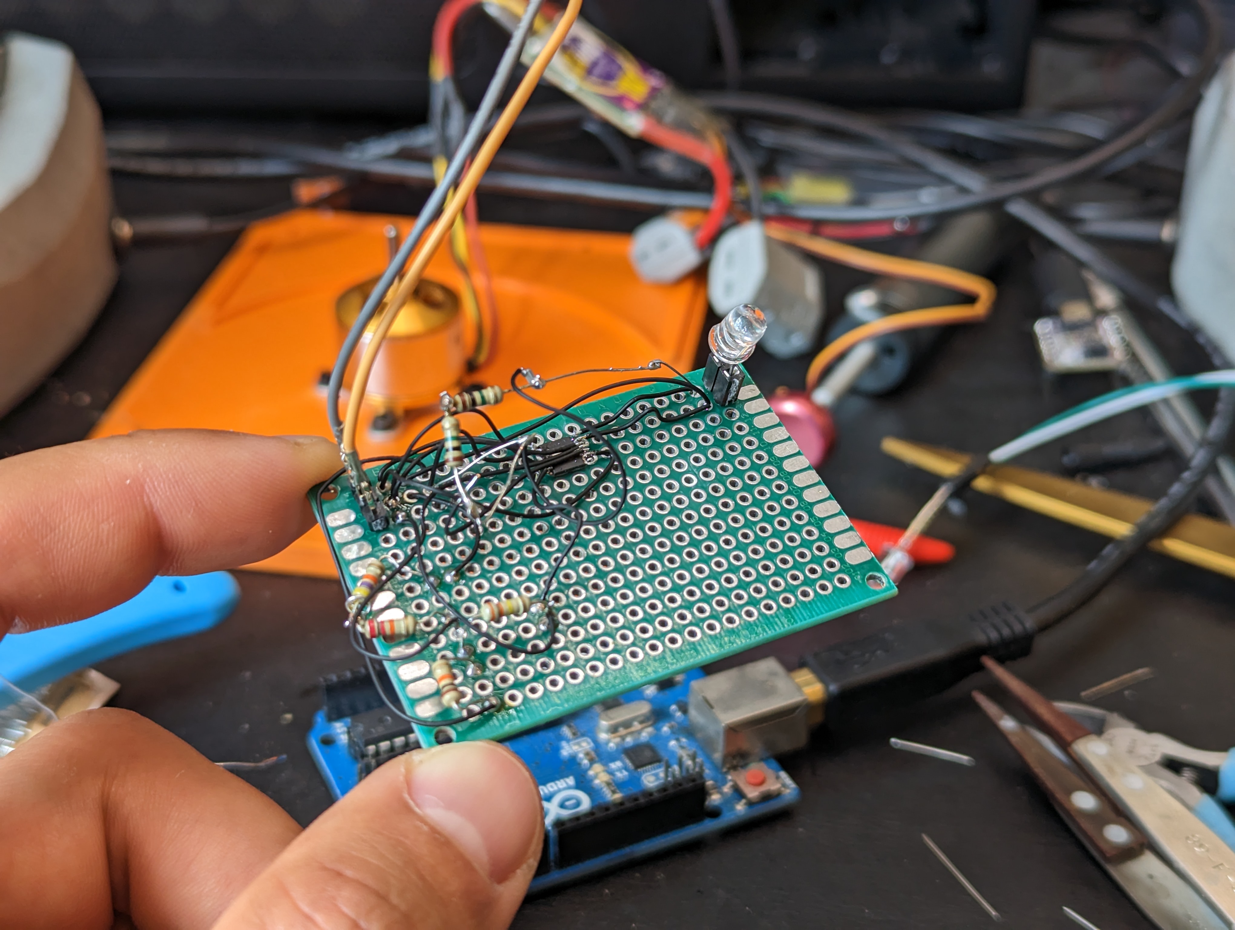
One component I don’t often use (aka have in the junk bins) are “fast” analog light sensors, like the kind you would use for a tachometer. However, I do have a lot of LEDs, and I managed to find one single op amp part in my junk bin, and so I figured I could either spend a day designing a pcb that would come in 2 weeks, or spend one day hacking together a tach.

My goal was to get a digital signal out of the system, where one rising or falling edge corresponds to one revolution of the motor. I want to run this motor from about 5-10k RPM, which means each revolution is 100 uS. Detecting something every 100uS is pretty slow in circuit land, so I was not worried about the speed of the electronics.

LED as a photodiode

I know that an LED can be used as a tiny tiny current source, and that there are two common ways to amplify it- with a transistor or with an opamp. I tried a transistor to start, since I knew I had some 3904s stashed away from an old project. However, this did not give me enough gain- the signal was only about 100-200mV with a bright light shining into the LED. I didn’t try the darlington pair, because later I found out I did have three (3) dual op amps in my junk bin.

I ordered three ALM2403QPWPQ1’s for some reason in 2021. I have no idea why, but I was pleased to find out that I had an op amp on hand. Fortunately, these are .65 mm pitch parts- that makes a big difference compared to .5 mm pitch parts for unaided hand soldering, deadbug style (note to self: buy microscope).

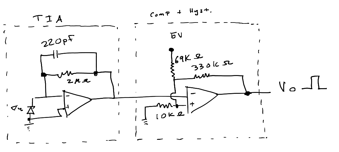
With these dual op amps, I could actually get everything I needed out of a single chip. The first stage is a transimpedance amplifier with the photodiode as a current source. This takes the current generated by the photodiode and turns it into a voltage. In theory it should be pretty linear with incident light, but I didn’t test this.

Since I have no idea where my LEDs came from (junk bin leds!) I just stuck in the values from the make article linked above (by Forrest Mims). This seemed to work well enough, but and testing showed that increasing the feedback resistor to 2Mohms gave me suitable gain, with an output around 1.5-2V. This signal gets fed into a comparator block later, so the actual value is not too critical- just that the signal has a wide enough swing.

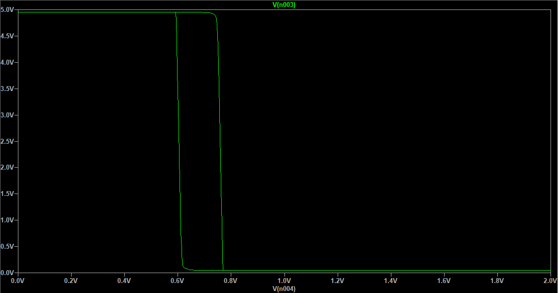
The comparator block is built out of the second op amp, resistors I had lying around, careful soldering, and this app note on adding hysteresis a comparator. I had to tweak the values to the resistors values I could make, but after some simulation I got a suitable result. Here you can see the .2 V of hysteresis in a plot of input vs output voltage.

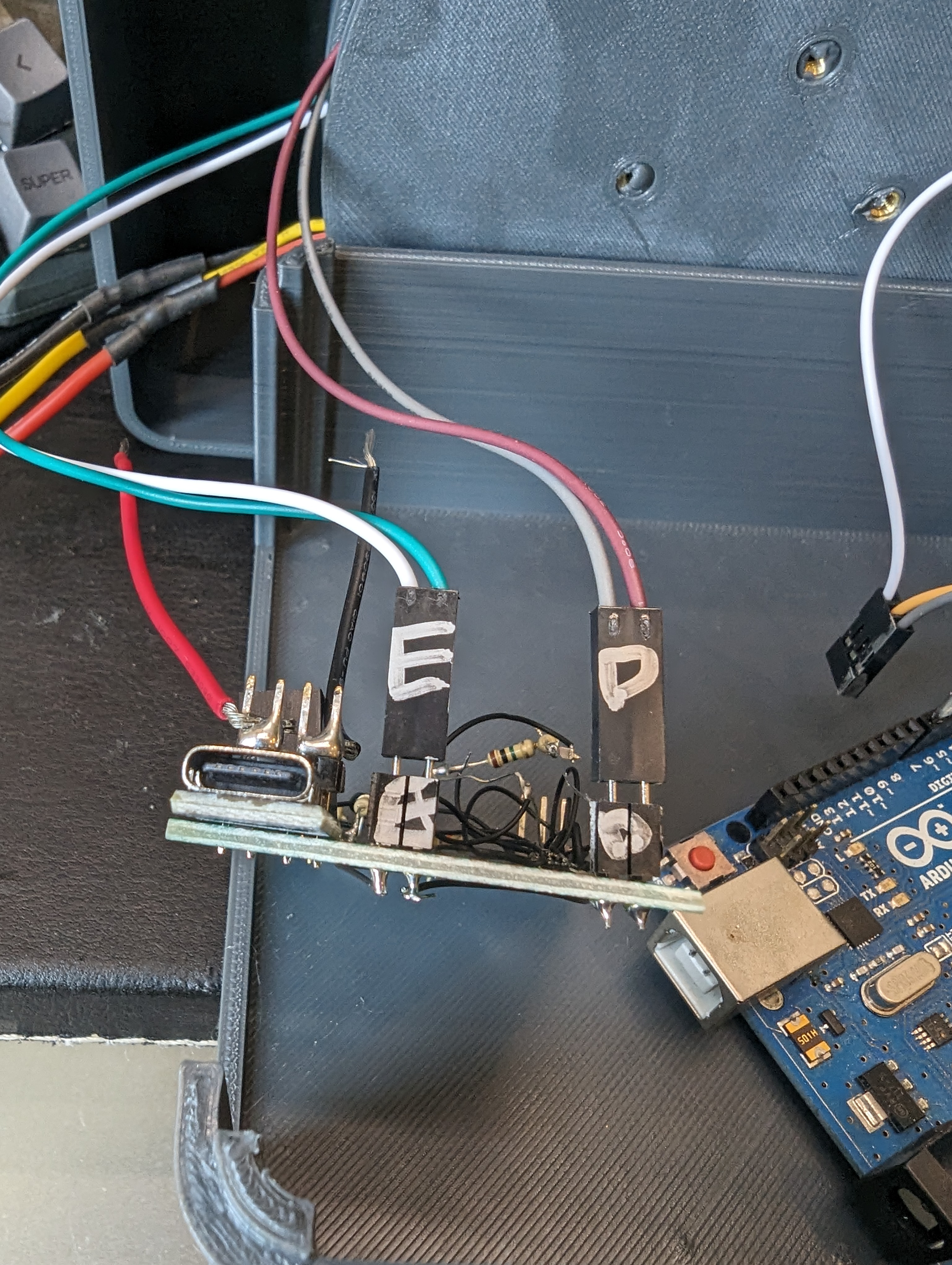
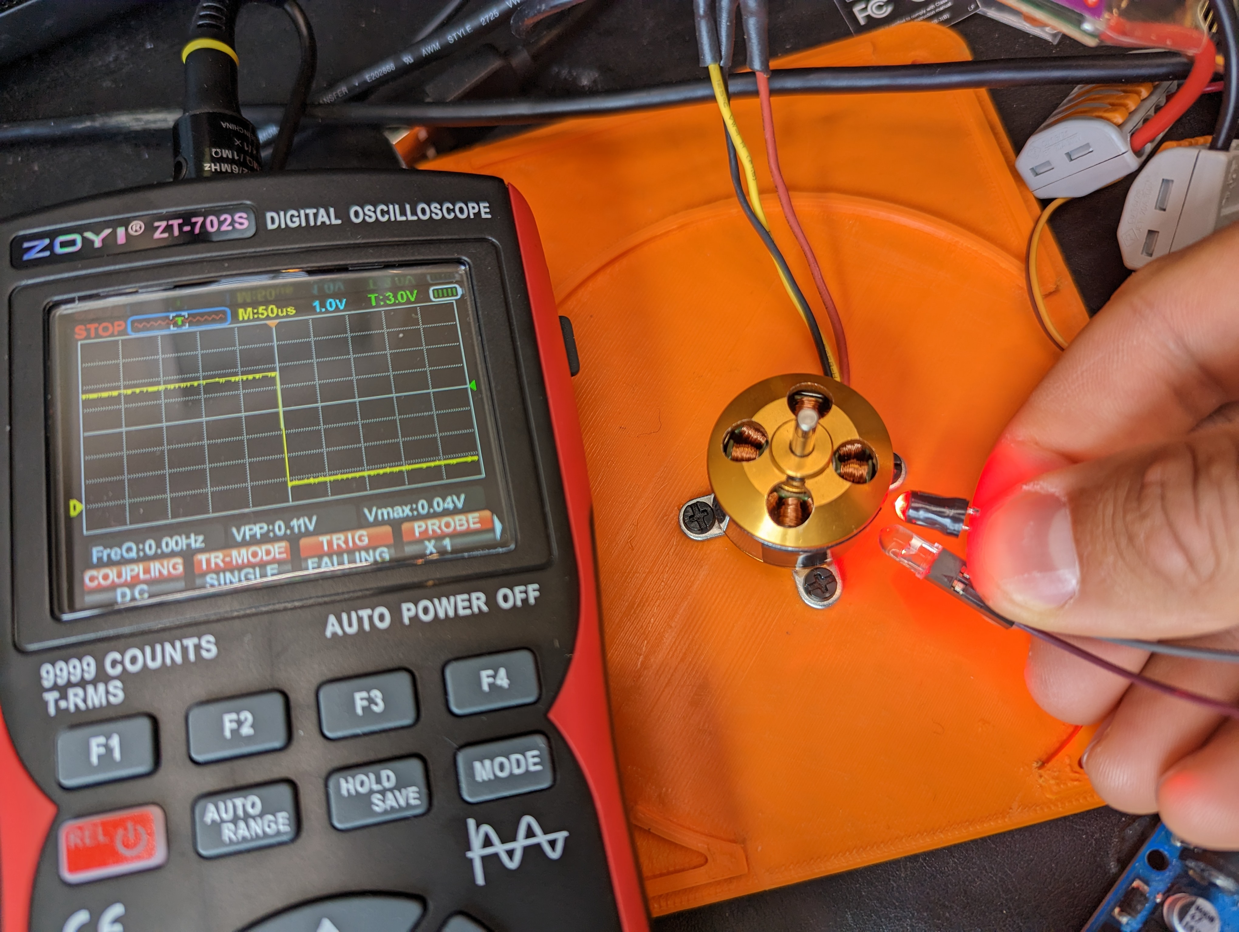
As you can see in the title photo, this produces a nice clean edge as the motor body (shiny) transitions to the tape (black, not shiny) that I stuck on it. Now its back to the mechanical drawing board to make a platformt to test/write software, and time to order a VERY simple PCB for when my questionable soldering starts to fall apart.

New Tool: ZOYI ZT-702S

A one new tool that made this way easier was the ZOYI ZT-702S. I bought this to augment my basic multimeter. I was skeptical of the oscilliscope feature after suffering through quite a few substandard scopes.

It turns out to be a total delight to use, and it is great for simple stuff like this where I want to look at some quickly changing value or to measure a rise time or to see if a signal is ok. It physically much easier than breaking out my big scope (because the big scope is VERY big). The portability also seems awesome- I have done all kinds of nonsense where I need to measure a sensor in the field and a multimeter is okay, but a very basic scope would be way better. This thing rules! It can even take screenshots, and the menus are straightforward.

My main gripe so far is that the auto range button exists- since its next to the hold button, I press it by accident sometimes and this resets my measurements and puts the scope in AC mode, instead of restarting the triggered data.

As a basic multimeter it also does fine, and the continuity beeper is very fast, and the probes are pretty nice. I am excited to add this to the toolbox!

USB-C to 300V Troubleshooting

In my last post I described the challenges in using the LT3750 as a high voltage power supply. Namely, the power supply needs to be restarted after it reaches its target voltage, since it is a one-shot “charger”. An additional problem is that when inspecting the output voltage, it didn’t quite match the calculated output.

Output Discrepancy

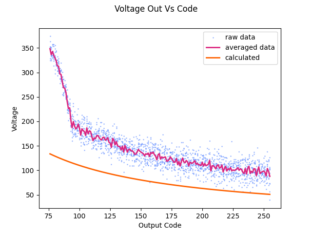
It was surprising to get this plot of expected vs measured output, as reported by the power supply. I would expect some scaling to be wrong, or to have some DC offset due to reworking the voltage divider with 5% resistors instead of 1%, but the hockey stick on the left side of the plot is pretty egregious. Not only do the values take off there, but the concavity of the line actually seems to change! This needed further investigation.

I actually didn’t believe it at first, but after verifying the plot with a few other instruments, and after testing the ADC, rechecking the voltage divider, and a lot of head scratching I realized the problem was in the LT3750, not in the rest of the circuitry.

This was puzzling because on the surface the circuit seemed to do what I expected, aside from the range of 75-100 counts (RBg max = 970 ohms). After scouring the datasheet, I realized that there is a limit on the current into the RVout pin of 1mA. This is not really highlighted in the datasheet. I had calculated a 12k resistor for Rvout in order to get a wide Vout range. However, this violated the rule for for Rvout, and my suspicion is that the proportional current source cant keep up, meaning Vrbg has a hard time overcoming the voltage in the vout comparator, resulting in an overshoot in the output voltage.

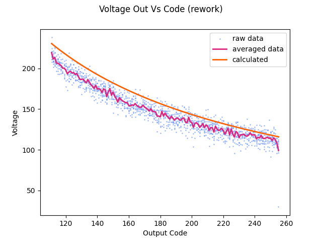
With this hunch, I replaced Rvout with a 27k resistor. This narrowed the usable output range by bringing up the minimum output voltage- ouput voltage is proportional to Rvout/Rbg, so its easy to have a higher voltage. Rbg is limited, per the datasheet, to 2.5k or less. This is annoying, since it would be nice to have a range from about 60V-300V, because my bench supply tops out at 60V. however, at the expected output voltage, the 27k resistor nearly limits the input current to 1mA, so it would be hard to go much smaller.

At least the output is sane now! Ultimately, I could introduce another digipot on the RVout side, but its probably not worth the hassle and the cost of another set of parts for what I want to do with this. The right way to get this power supply might actually be to just use something with continuous feedback to avoid having to kick off another charge cycle.

Output Accuracy:

With the output related to the input, the next step was to relate the potentiometer codes to output voltage. Sadly, this needed to be compared to some instrument, and my multimeter does not have peak hold. So I hooked the supply up to my scope and measured the peak voltage (for a few cycles) per code. I know the expression for the output code is:

Where B is the terminal resistance/parasitic resistance of the digipot (Rbg), and A is a bunch of stuff (turns ratio, a constant, the Rvout resistor value). It doesn’t matter since I am just fitting this curve. The parameters A and B were extracted with scipy, and plugged back into the control code to control output voltage.

Improving ADC reads with rp2040 PIO:

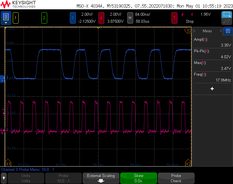
The output stability was initially very bad. This is because the sampling was running very slowly- even running on its own core, reading/writing GPIOs and evaluating expressions takes a lot of time- here you can see the clock rate into the ADC was only 6.7kHz- much lower than the minimum 5 MHz. To put it in perspective, the raspberry pi is only running 6x faster than the max speed that that the adc can be sampled. The slowest sample speed would allow 25 instructions per- reading, including whatever is needed to generate the PWM.

Even at high speeds, it takes a lot of time to get a good sample. Since the output is a bit at a time, each bit only carries one bit of information- this sounds obvious but that means that to get a typical 8 bit resolution, we don’t need to sample 8 bits, we need to sample 256 bits. even running at 20MHz, that still means only one reading every 12.8 microseconds, and that would give worse than 1 volt resolution.

In theory, with proper filtering (which I’m not doing), the adc can provide 16 bit resolution, which is incredible. I decided to settle for taking 12 bits of samples and decimating them, running at about 18 MHz for about a 200 microsecond conversion time (plus some small overhead).

This required using the PIO of the RP2040. PIO is super cool- its like a teeny tiny extra microcontroller that gets run with a tiny(!!!) 9 instruction set. This instruction set is extremely limited- even more so than typical assembly. For example, you can do something like load a number into a 32 bit register, but you cant load a number that is bigger than 31. There is no automatic incrementing of registers, but you can decrement some registers using the jump command. Its a beautiful, but strangely functional (and very fast) mess.

Basically what my code does is load a counter into the y register of how many pwm cycles to do, and loads the maximum number into the x register – 0xFFFFFFFF. Then it starts clocking out pwm cycles, and uses the jump instruction to decrement the x register and y register. When the y register is empty, it reports the x register back to the main program and restarts.

With a little math, this results in how many “high” bits there were in the data. This duty cycle is related back to the read voltage through some simple math from the AMC3306 datasheet and the resistor divider information. This tended to read really high at low voltages (20V when the output was shorted), so I added a correction/adjustment factor to bring it back in line with reality.

Output Stability:

I wanted to get a very rough idea of the output stability. It’s not easy to to claim any kind of stability or even claim a power output without a variable load of some kind, but I wanted to at least be able to set an output voltage and look at how the supply can regulate against the internal bleeder resistors.

Overall its not too bad- the max is within a volt of the setpoint, and the ripple seems to be about 10V, although given the resolution when zoomed out this far on the scope I am not totally confident in that. Given the hackery and amount of new stuff that went into this, I am satisfied with the outcome.

What I would change:

In the scheme of things, this project went pretty well- I tried at least four or five new processes, so anything working at all is a small miracle. However, there are a couple things I would change if I did it again. Here is a very public bug/ wishlist:

Indicators for hazardous voltage presence, CHARGE and nDone would be neat and blinky. Its nice to have activity indicators. I could actually add most of these with some rework, but it would have been smart to put them on the board!

I do have provisions to add an I2C screen, but no real plans to use it at the moment. This is another nice to have, to get feedback instead of using the console or a dmm, which is limiting. Originally I didn’t expect to use the feedback delta sigma modulator, so this information would not have existed in the system. Now that I have it, it seems silly not to display output voltage.

Increasing the allowable output voltage would also be easy with a substitution of output diode and output caps. It would be wise to choose output caps well in excess of the possible output voltage- even at the expense of space. Currently, my power supply can be commanded (accidentally) to self destruct!

Obviously it would also be great to go back and add the right parts for all the r’s and c’s that are bodged in.

Fix the feedback divider for better range!

PIO errata:

side loading is awesome! it basically allows you a free instruction to set output pins while you do other stuff. The “other stuff” I am doing is nopping, but this could be super useful.

labels at the end of your code will get optimized out. even if they have a nop()[x] after them. however, a regular nop() will keep them in the code.

adc pins used in the pio need to be explicitly enabled in the way you want, e.g. pin = Pin(28, Pin.IN) or pin = Pin(28, Pin.OUT). The PIO state machine class will not do this for you.

Micropropagation of wild-type Vaccinium Vitis-idaea

A few years ago my friend introduced me to a tasty and edible berry while we were on a hike up mount Washington. I had no idea what it was, and much later I learned that they were lingonberries, which are related to a lot of other shrubby berry plants like blueberries.

Recently I learned that plants are very sneaky and do not always come from seeds. In fact, most plant cells seem to be totipotent (capable of creating any other kind of plant cell) and capable of creating undifferentiated cell mass (callus culture) if you feed them the right stuff. I had previously considered a plant (particularly woody plants like trees) to be single monolithic organisms with parts that fall off that are dead/not useful. It seems like it is more the case that any part of a plant can turn into another copy of the plant, under the right conditions. Think about that next time you are looking at cabbages in the supermarket.

It turns out that most ornamental plants, and many commercial plants are grown not from seed, but basically from cuttings that are carefully grown in lab conditions to maximize growth and multiplication of the plants. This is called micropropogation, and its useful for getting (usually) genetically identical copies of plants. This is helpful for preserving desirable mutations.

You can probably see where this is going: tasty plant + new technique = a small project that will likely take many years to complete. I want to grow our local variety of lingonberries!

Media Prep:

these blueberries were growing right on top of the lingonberries!

After weighing my options on media I decided to go with a media that was actually recommended for blueberry bush micropropagation from “Plants From Test Tubes: An Introduction to Micropropagation”. While there was more specific media recommended in some papers on propagation, it was not clear to me (as a neophyte) that “modified ms media” was actually a specific modification of MS media, not MS+2ip. It was possible to have ordered that media, but a lot of items were backordered for months, so I ended up with regular MS media, and 2ip. At this point it was too late to get the specific modified MS, and blueberries and lingonberry plants grow right next to each other in the wild, so it seemed like it might work.

The media I made was not exactly per the book either, since I think my MS mix already had inositol. The final mix for initiation media was:

  • 1L distilled water
  • 2.3 g MS basal media
  • 5ml 2ip @ 1mg/L (roughly .25 umolar)
  • 20 g sucrose (refined white sugar)
  • 6 g agar

The 2ip concentration was in line with what I had read was ideal for initiation from Jakkola et al. 2001, which was encouraging. The media was not checked for pH since I didnt have a meter or strips, but I would have liked to adjust it down to 4.8, which is a reasonable pH for a lingonberry plant.

One nice thing about this media is that it does not seem particularly rich (surprising given the sugars). I intentionally exposed a plate to contaminate it and it took weeks for some mold to show up. With LB, I would have expected it to be disgusting almost immediately.

Explant Collection:

Explants were collected from a population near the alpine garden trail on mount Washington. only a few grams of plants material was collected over about a hundred yards of trail, in order to minimize impact on the environment. Explants were stored in sterilized falcon tubes for transportation.

Explant Preparation and Plating:

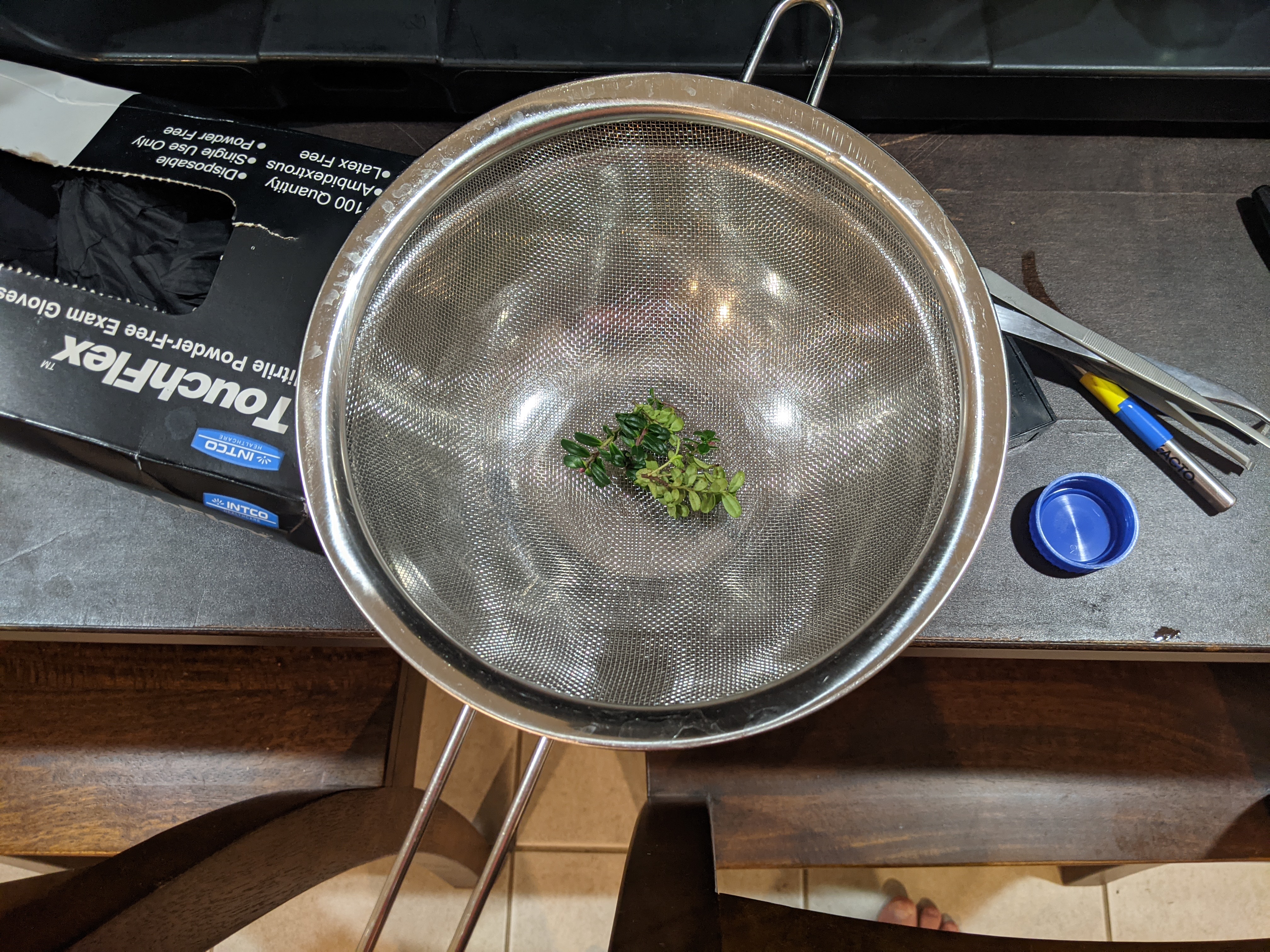
Explants were placed under running water in a strainer with a bowl beneath it in order to create an agitated water bath. The plant tissue was washed for 10 minutes under running water to remove dirt. explant material was then sterilized in 70% IPA for 30s, and then washed in 1:10 bleach solution for 25 minutes. a drop of dawn soap was added to the bleach as a surfactant. After sterilization, the plants were washed three times in sterilized water.

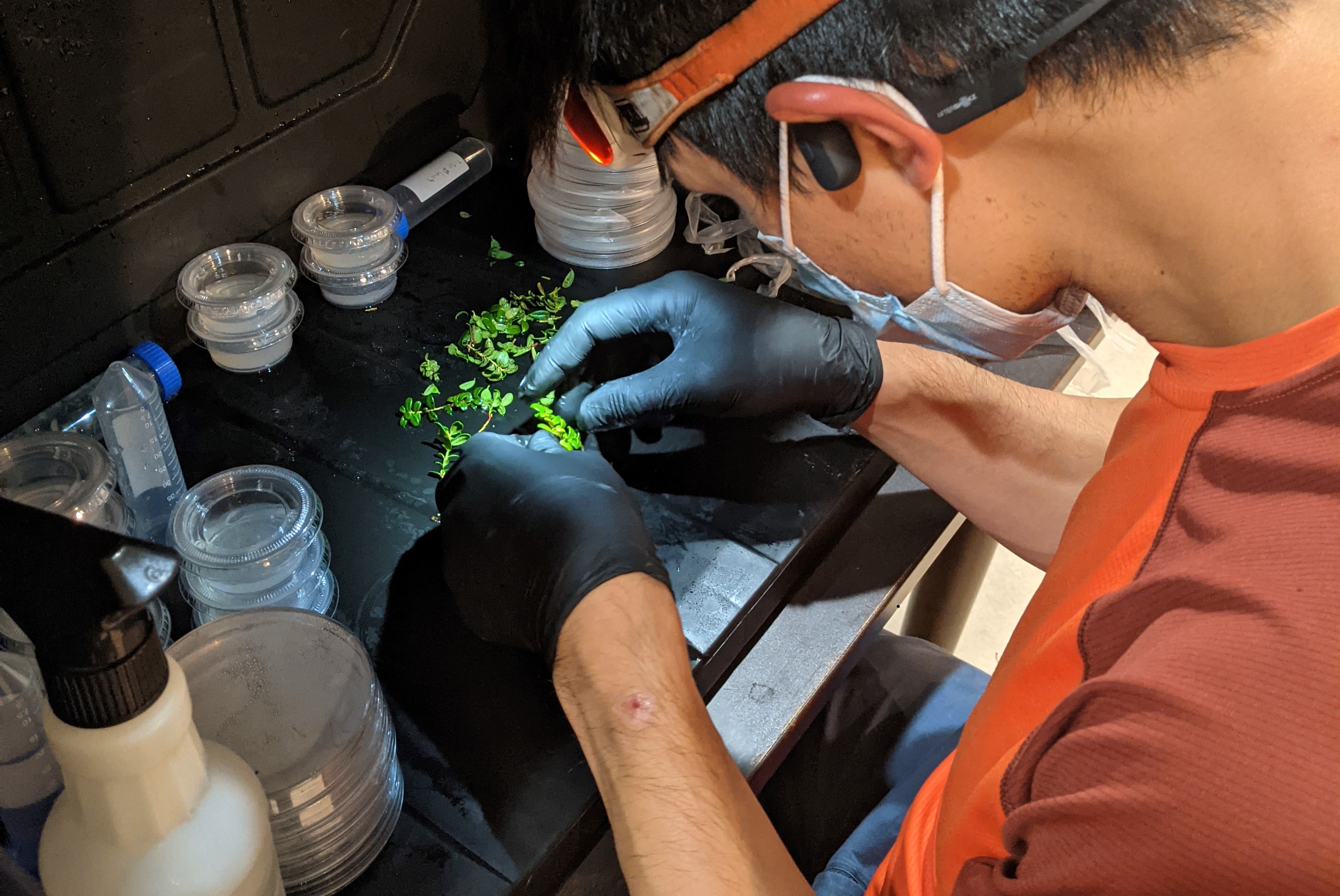
Plants were handled inside of a plastic bin that was sprayed regularly with bleach solution. Tools were sterilized/stored in bleach as well in between uses. I would recommend a clear bin for better lighting. It was challenging to cut the plants in a dark box, but after roughly three weeks, there was only one obviously contaminated sample.

Results

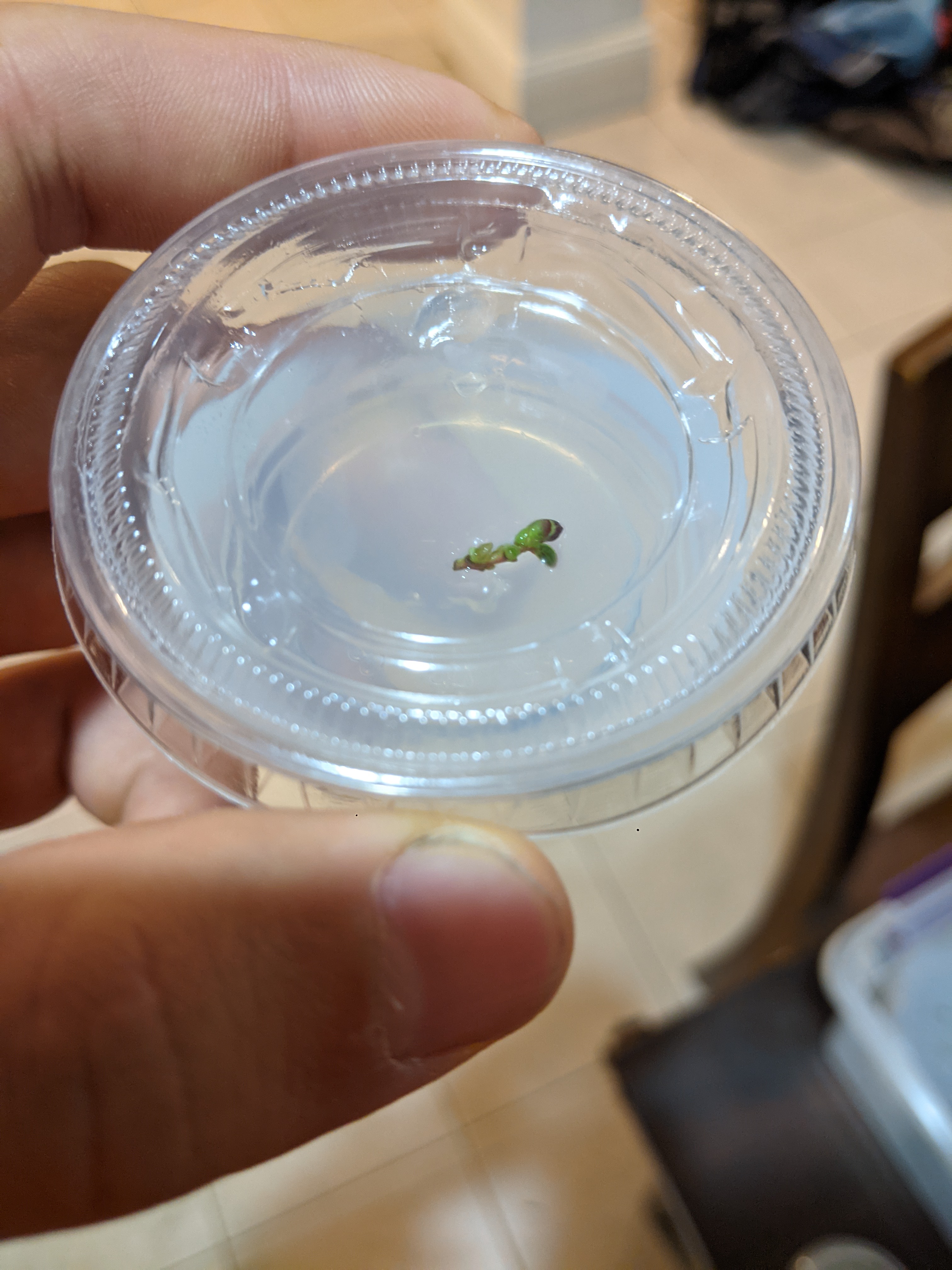
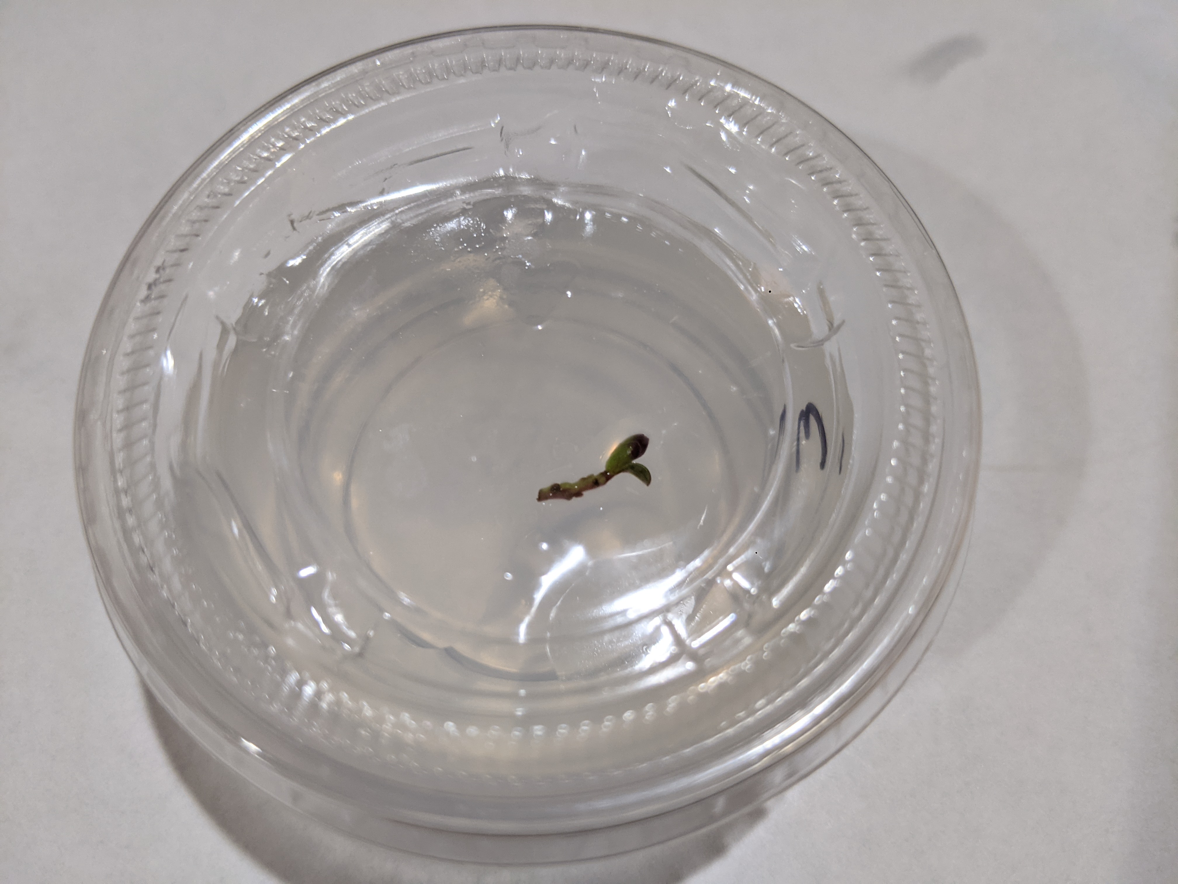
I’d like to call this section something more optimistic, like “success”, but I never really got anything to root. However, there was evidence that the media is sufficient to support the plants. In the photos above, the left photo (with new leaves) was grown from the small browned sprig on in the right photo. The right photo was taken on October 5, and the photo on the left was taken on the 19th, two weeks later. New leaves are clearly visible, and it seems like the plant is producing chlorophyll.

I’m not sure if this is strictly useful, but the lack of contamination and the plant being alive is a good first step.

Adjustable High Voltage USB PD Power Supply

A usb-pd that nobody wanted or asked for. However, I needed one.

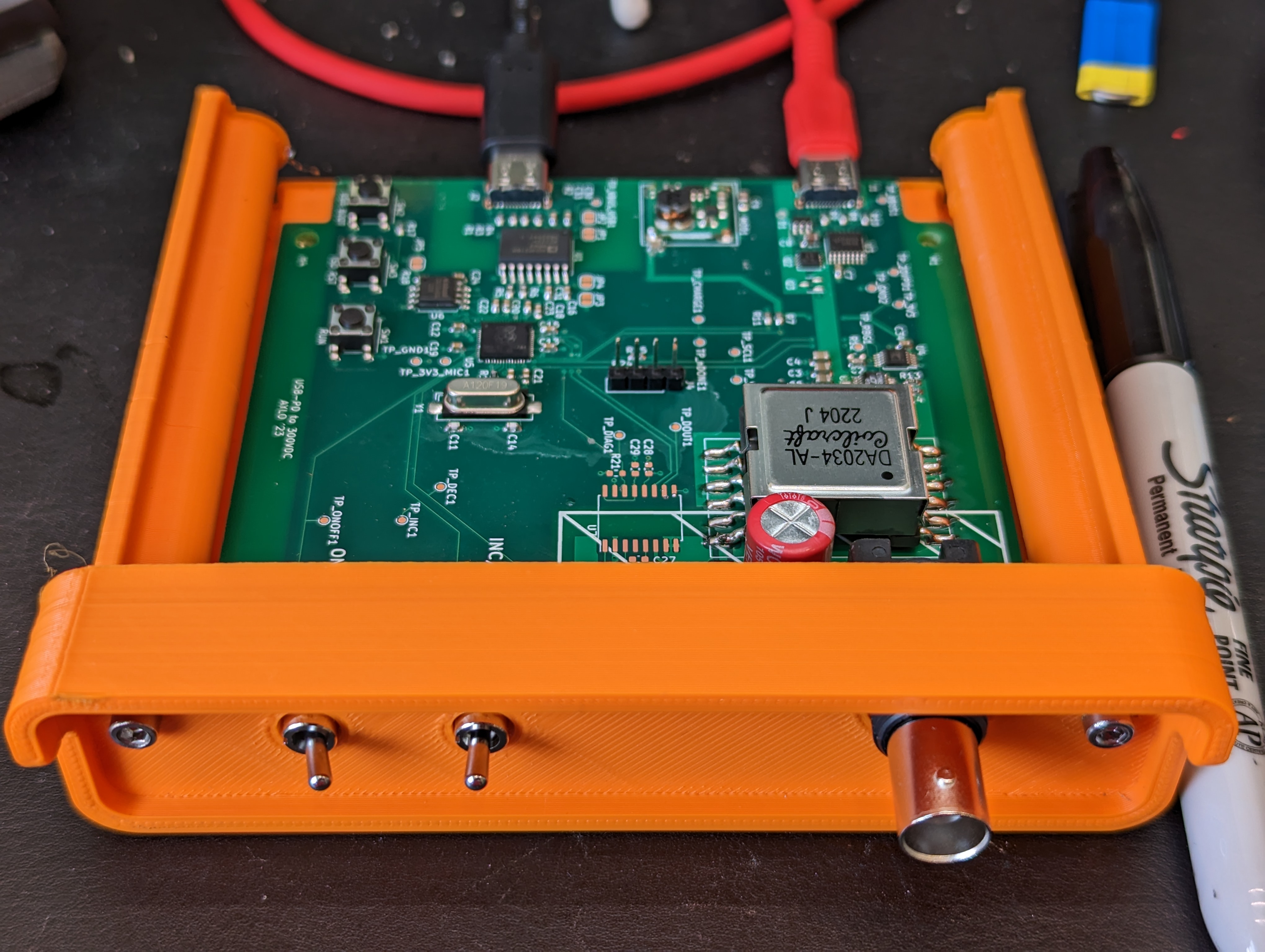
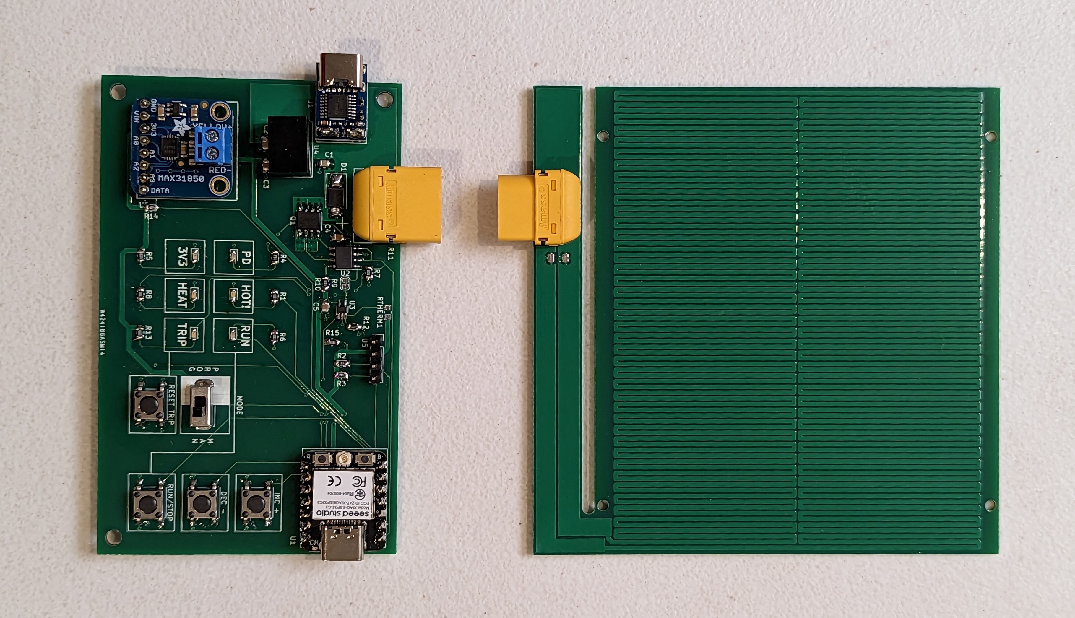
When I say high voltage, I don’t mean 20V, I mean around 300V, for high-voltage DC needs like electrophoresis or electrowetting. This is a gratuitous and impractical project, since you can buy an electrophoresis power supply for about $100. However, I wanted to do a more compilated design, and I “needed” a test PCB for my hotplate, so I made this.

The goal of this project was to make something worthy of being a lab instrument, e.g. not completely unsafe, and not held together with string and gum. I want to “have it all” with this instrument and even more than that I wanted an excuse to use a lot of new parts and tools.

With respect to safety, I wanted to essentially live up to a standard of a double insulated tool- that anything conductive sticking out of the case (unless it is live) has double or reinforced insulation. To avoid USB ground loops or accidental ground-referencing due to an evil USB port (or a short of shield to ground), all USB ports are isolated from each other and from the high voltage.

In short, in addition to this project being impractical, its also somewhat risky in terms of project bringup- it was possible I missed something or that a circuit just won’t work and would be impossible to fix.

High Voltage Generation

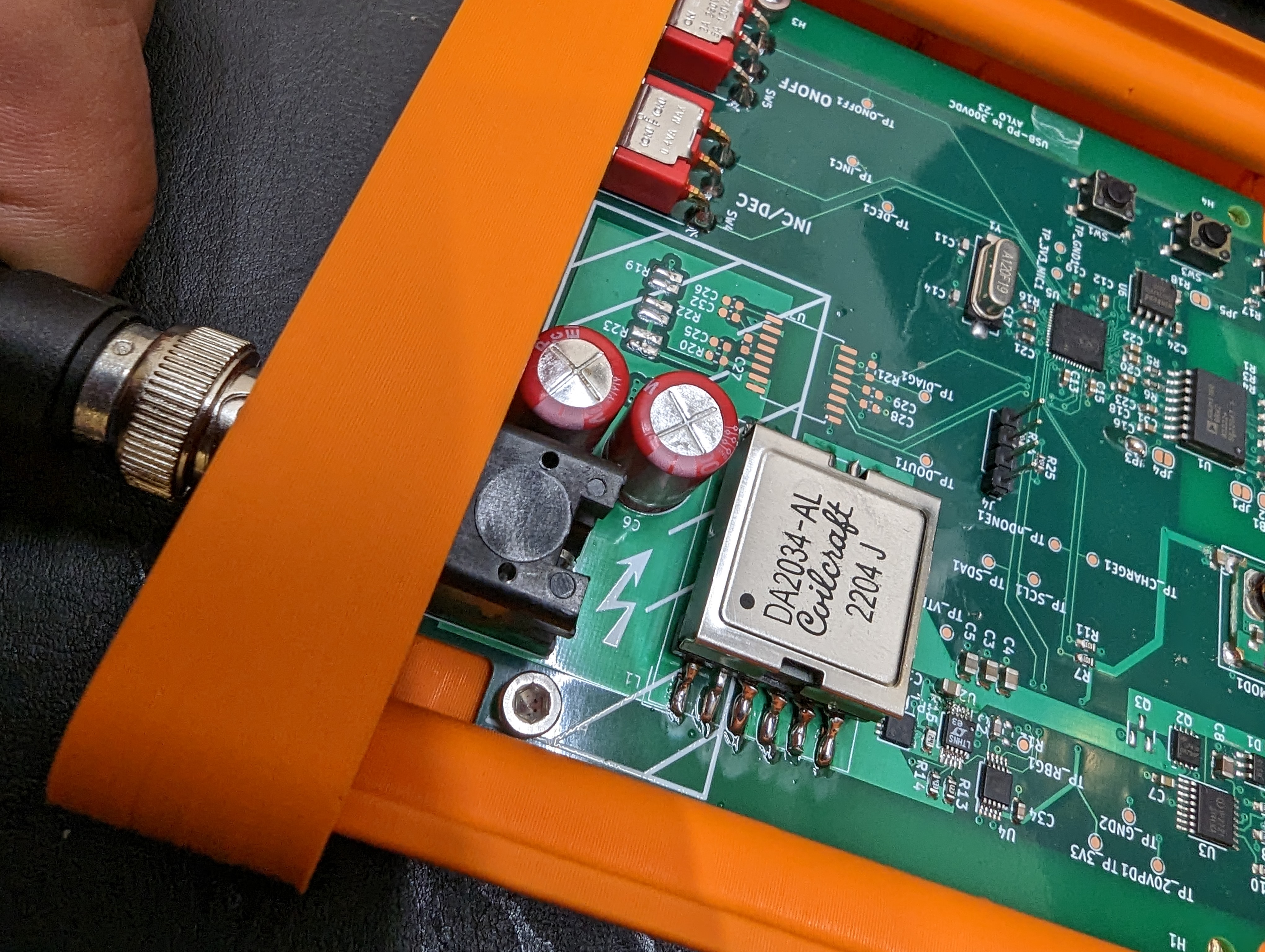
Ignore the loose solder blobs…those got cleaned off.

I wanted to use a flyback converter to take advantage of the inherent isolation of the transformer. The 300V out is not ground referenced, which makes it a lot safer since you have to touch both wires to get zapped (this will hurt). To maintain isolation, the output voltage cannot be sensed directly (with a conductor). One option is to use an opto isolator, but that requires more board area, cost, and things that can go wrong.
Another option is to use a flyback controller with “PSR”. PSR is primary side regulation, which senses the voltage induced on the primary while the secondary coil is discharging. This cleverly uses the transformer itself to avoid extra parts or breaching the isolation. There are a few controllers with this feature.

I also wanted the flyback to be adjustable- this is not as easy since it seems like these controllers are most often used when “just one” voltage is needed over and over again (many are for charging photoflash capacitors). The trick was finding one where only one resistor value needed to be changed, which I could do using a digipot.

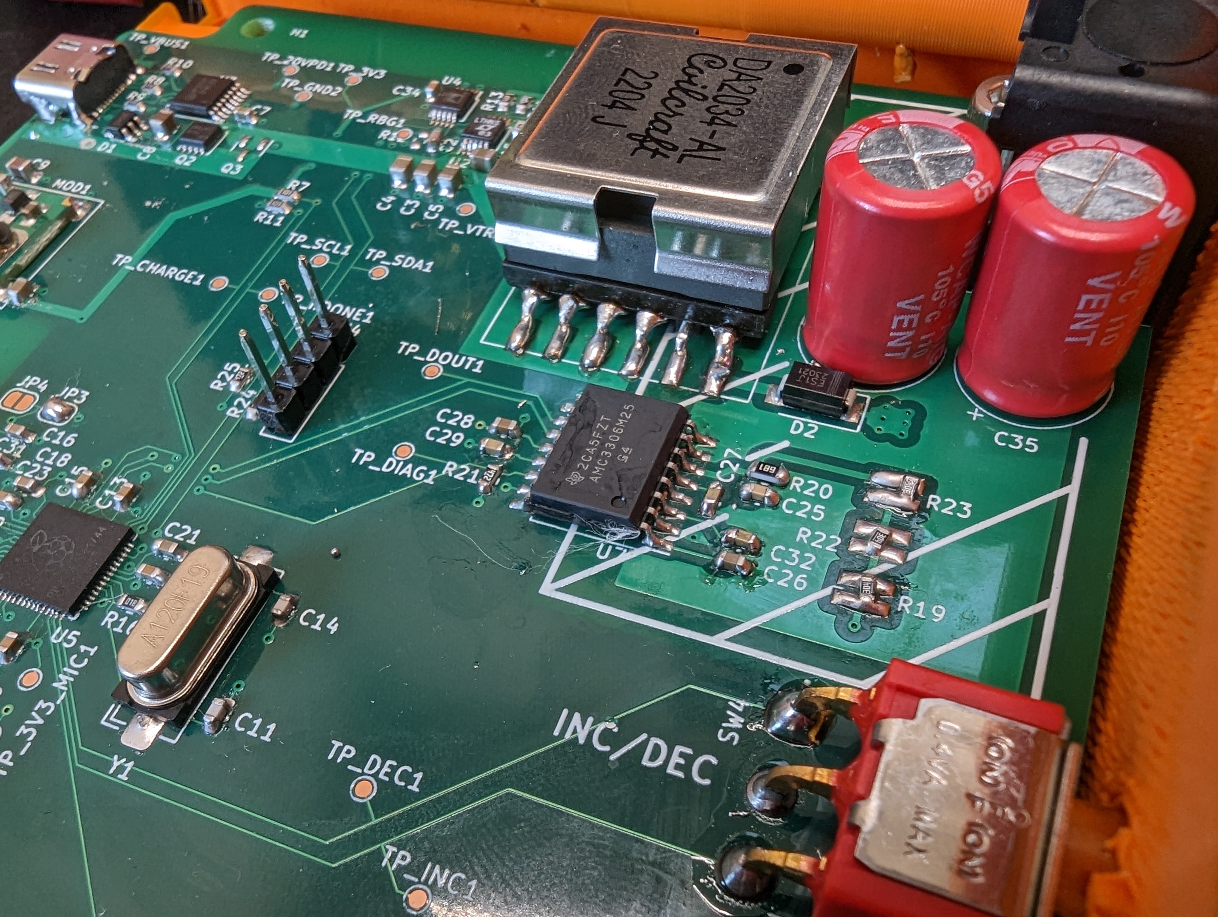
I landed on the LT3750, which checks all the boxes. An additional factor was that coilcraft sells a special inductor that plays nicely with this controller, and for my application which has very high primary side currents (low DCR), low leakage inductance, and needs a relatively high inductance to be slow enough for the controller.

For safety, I added a high value bleeder resistor to the output caps, so they will discharge below the hazardous voltage threshold within a minute or two of disabling the supply.

N.B.: I later figured out that choosing a controller without continuous feedback was a problem- I made it work but its not ideal, see what went wrong.
USB Isolation

This device has three ports- two USB and one BNC. It’s important to prevent any conduction from one port to another, to avoid ground loops or ground referencing. The power USB port is isolated from the high voltage by nature of the converter. The data usb port (also for programming the RP2040) also needs to be isolated from the power USB port.
To do this I used an ADUM3160 which is a full speed, reinforced isolator. this provides a great deal of protection from voltages on either side of the isolator, which is important to protect both myself and my computer!

This worked off the bat at full speed, with little care given to the trace lengths/impendence ,since I kept them short. Surprisingly, the main design issue in the whole project was using the wrong jumper footprint, which left the device speed undefined on the rp2040 side. a single blob of solder fixed this (shown above).

RP2040

At the heart of this all is an RP2040. I’ve never used one of these (or micropython) but they have a pretty good hardware design guide and it looked simple enough to one-shot the design. Surprisingly, soldering the QFN went smoothly, and the usb bootloader worked flawlessly, which is an unusual and totally delightful experience.

Bringup with the RP2040 has been similarly delightful- using the REPL, its easy to query devices over I2C and to make sure that all my buttons etc. are hooked up correctly in only a few minutes. It was also easy to write scripts to quickly test the power supply. I can see a lot of reasons to use this in the future.

What Went Wrong + The RP2040 is a Hammer

The LT3750 has PSR, but no feedback about what the voltage is unless it is charging. This means that if it is charging, it is regulating the voltage, and if it is not charging, it has no idea what the output voltage is. Checking what the output voltage is can only be done by pumping a little energy into the output and seeing what happens, which increases the output voltage (if done frequently).

Days since magic smoke released: 0

To maintain the output voltage for different loads, the output needs to be checked frequently. This checking can easily drive the output voltage up (based on the minimum resistor value, to about 600V), which is enough to blow up the output caps, fry whatever thing you were running off the power supply etc. – in short, its nasty.

If not checked frequently enough, the output voltage will sag under different loads. What works for maintaining voltage across the bleeder resistors might not work for a real load.

Fortunately, I had planned to use the AMC3336-Q1 to measure the output across the isolation barrier. This part is super convenient to use because it is powered from the isolated side through some integral magnetics. This eliminates needing to do funny business to get a low voltage source referenced to the high voltage side.

Sadly the AMC3336 was out of stock, so I ended up with the AMC3306m25. This is the same part, but it only has a 250mV range, which is ok because that only required a small change in the resistor divider.

By using the AMC33X6, I can measure the output and kick on the converter if the output drops from within a few volts of my specified output.

One annoying thing about the AMC33X6 series is that the output is fairly high frequency digital output. The output is basically is a 5-20Mhz square wave that needs to be measured synchronously with a CLKIN signal that also needs to be generated (at least on my board) by the micro. The digital output actually encodes raw ADC information in terms of duty cycle. The proper way to process this is with a digital filter (and who knows- maybe I’ll do that) but currently I am just decimating (averaging) it.

If this sounds like a job for some low level micro peripherals, you are right. Or if you think this is the perfect application for the raspberry pi PIO, you would also be very right. However, the rp2040 also has an entire 125MHz core that I wasn’t using, so instead of doing it the hard way, I did it the easy way and used the second processor to generate the clock signal and to read/process the data in.

This works reasonably well, and I’m ready to start developing the rest of the application for which I need this high voltage supply.

Source

If you are interested in any of the specifics of this project, you can get the source here.

Hot Plate Usability Upgrades

My hotplate, while very functional, was not user friendly. It was a small matter of software (SMOP) to solve these issues.

The buttons work!

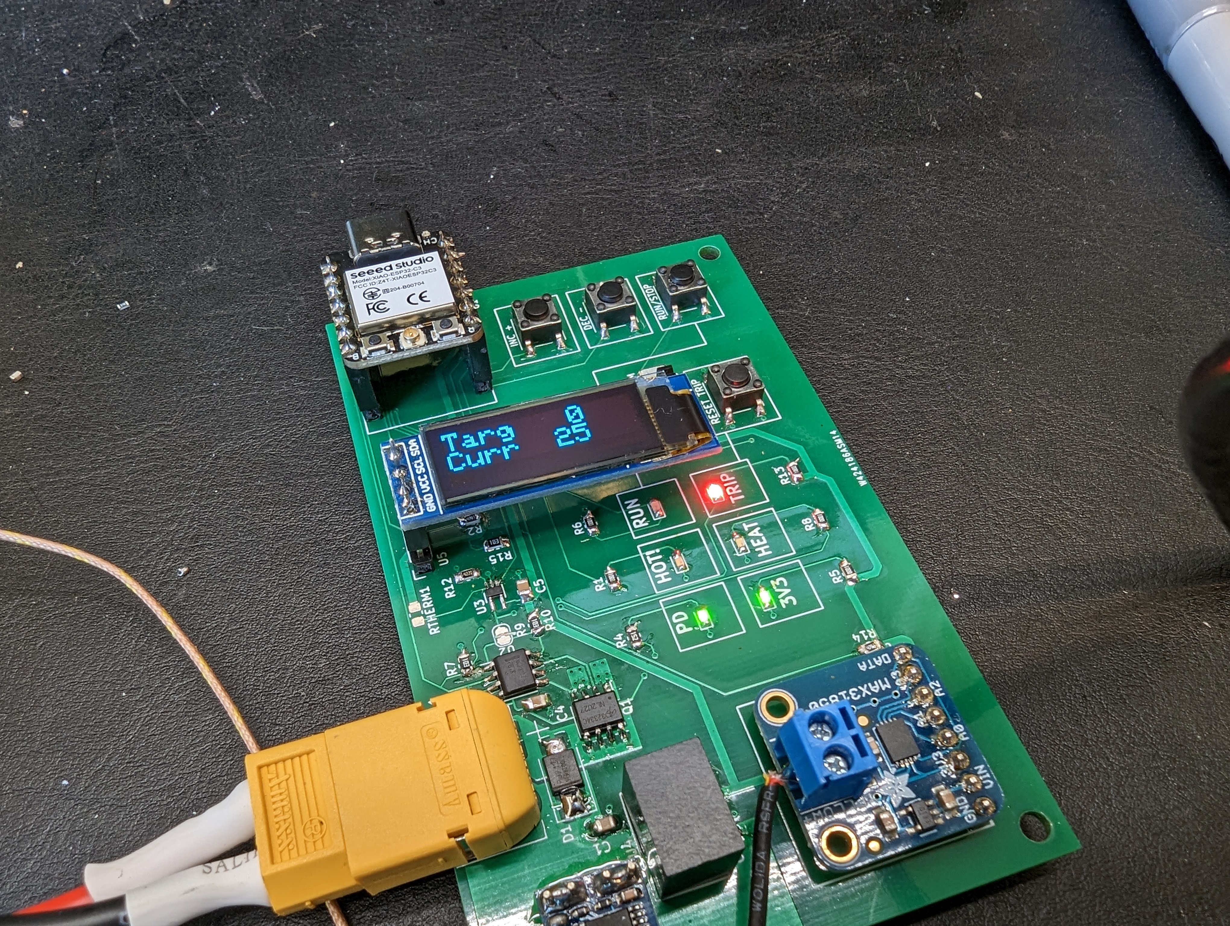
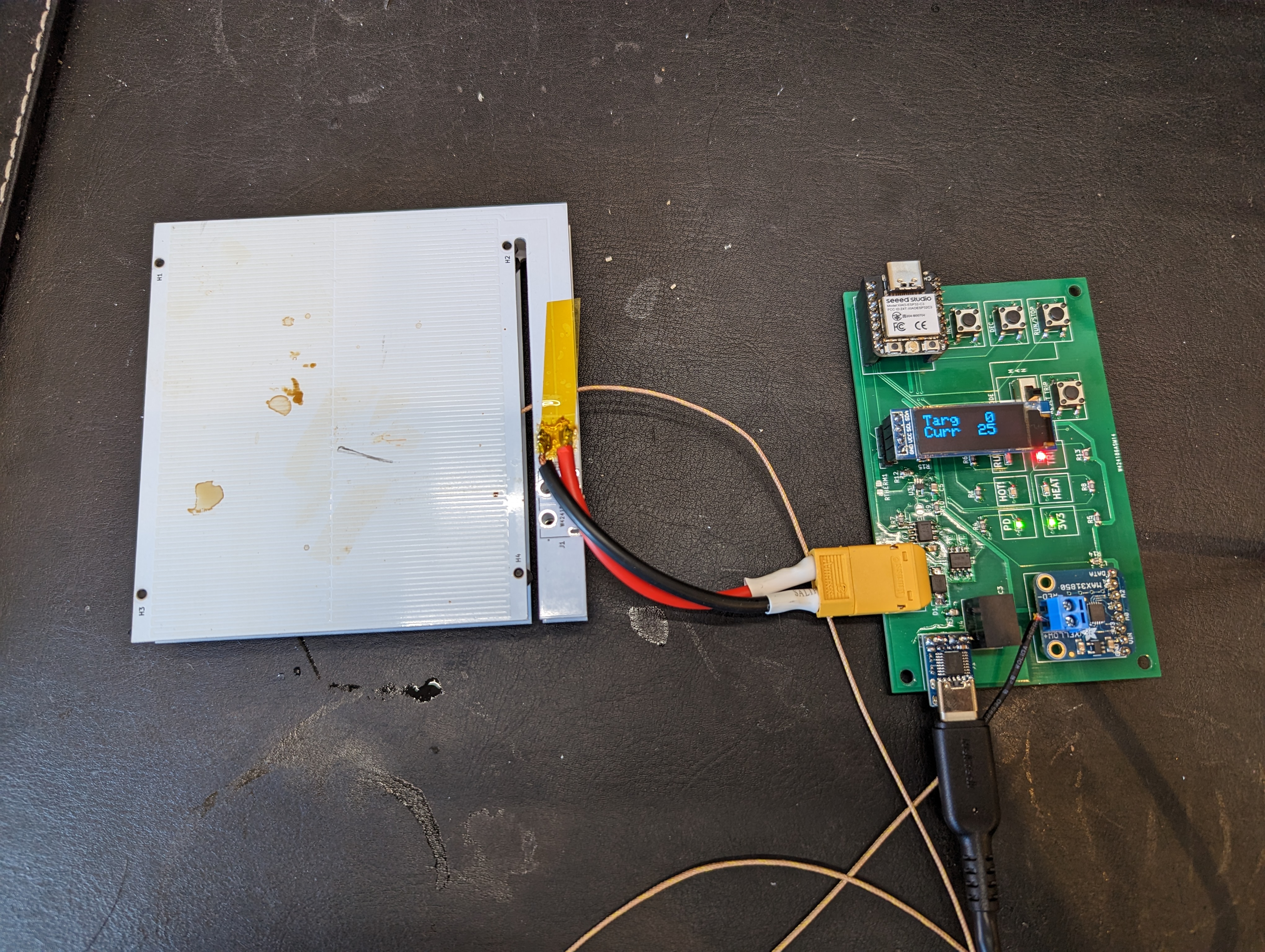
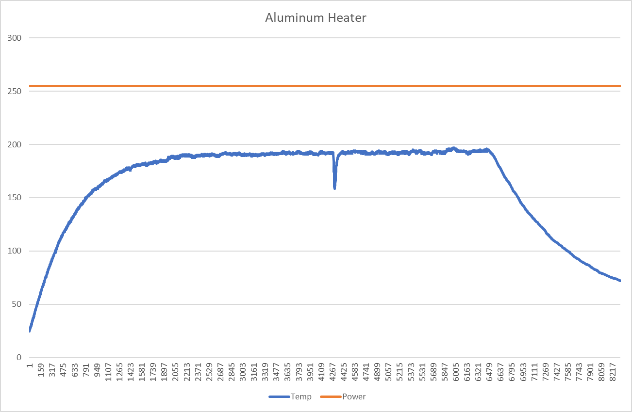
The hotplate can be turned on and off and controlled in increments of 10c using just the buttons. This frees it from needing to be hooked up to the computer with another USB cable. I originally imagined that having computer control would be neat (and it would be), but its not really necessary for anything that I am doing right now, and it impedes my workflow to do so.

There is a screen!

This screen really would be better off rotated 90 degrees. the final hotplate controller will have that, but for now I will just have to use my imagination. This screen is at a funny angle because the original plan was to control this through the serial port and specifically not to have a screen.

To Do:

This thing needs some kind of case, both to protect the electronics and to make it easy to use and store. I will probably 3d print some kind of temporary mounting arrangement, and also spin up a finished version of the user interface. That UI will probably get assembled on the hotplate!

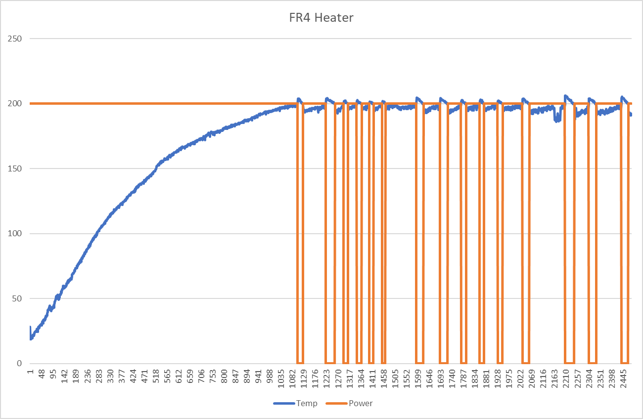
Tin Bismuth Solder + PCB hotplate

My first SnBi soldering project

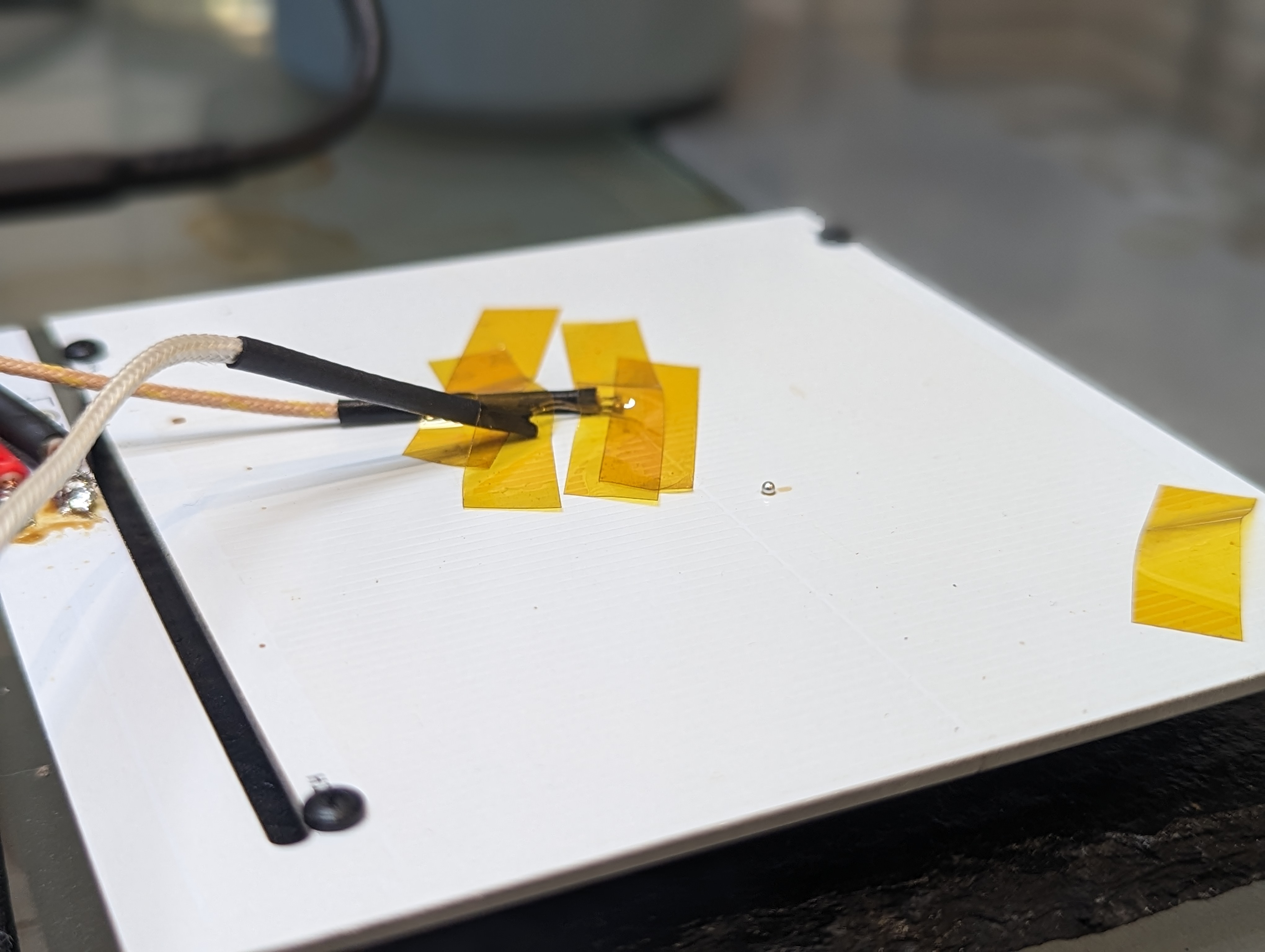
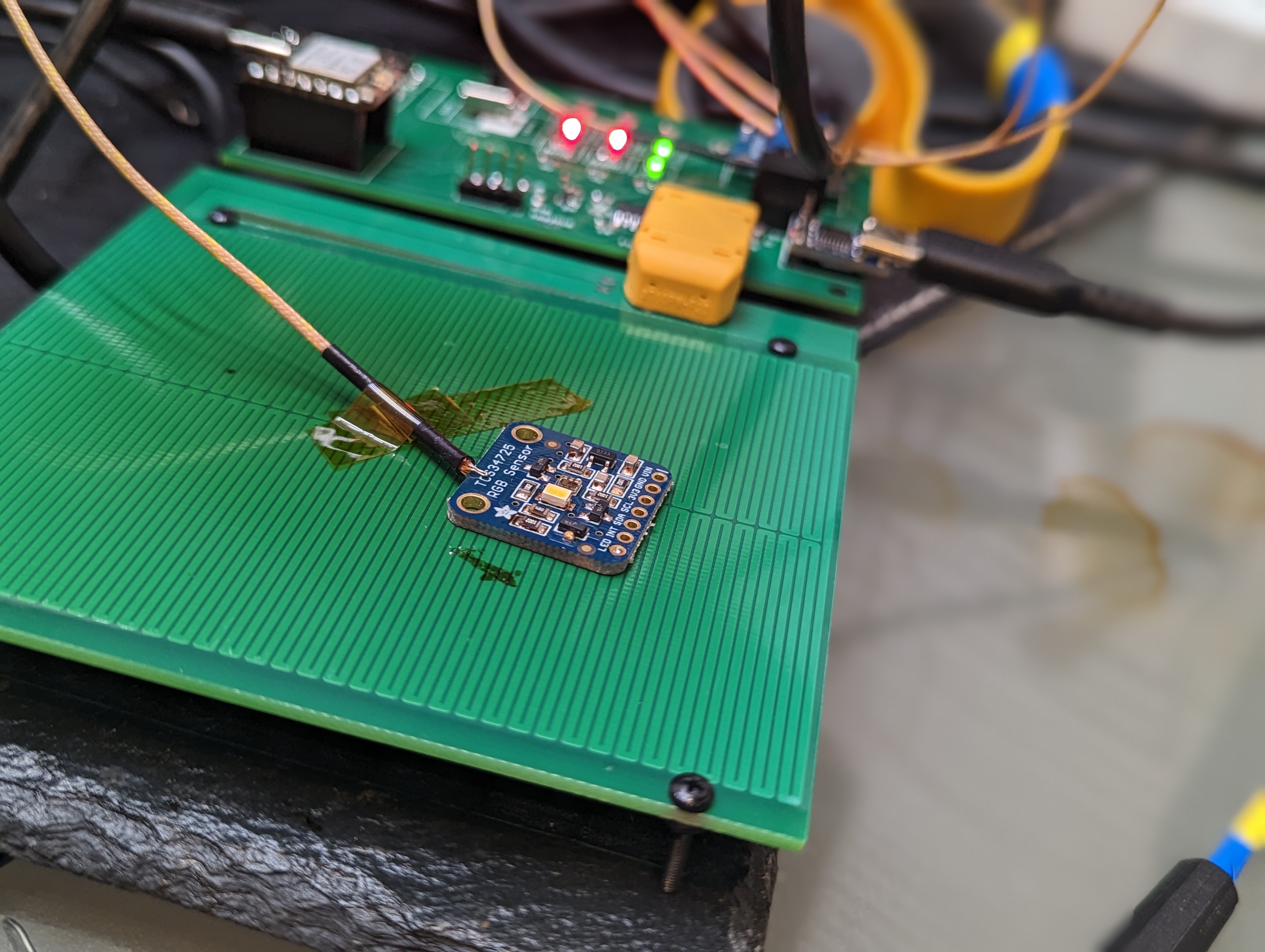
With my pcb hotplate built, I needed a test for my new tool. My goal is to be able to easily do prototypes of pretty much anything in-house, to avoid the delay, cost, and general PITA of outsourcing board fab. I also want to switch to a lead-free process.

Motivation to go Lead-Free

There are a couple of advantages I see with moving to lead-free SnBiAg solders, especially at home. The first is that the liquidus temperature is much, much lower- around 140 C. Eutectic tin-lead solders come in around 185C, and SAC lead free solders melt around 220. This lower temperature has two pleasant benefits. First, you won’t end up scorching your parts/silkscreen/soldermask with hot air trying to get some chip off the board. Second, everything is easier/faster to heat up since less energy is required.

This lower temperature also seems like it should reduce the energy in the flux fumes, which I can only assume is better than the alternative (use a fume extractor, kids).

The other advantage is that there is no lead in lead free solder. It’s 2023- we know lead is bad. I have done a lot of soldering with lab/food separation, and while leaded solder is probably fine if you have a lab setting, its not something you want to get in your carpet/personal desk/place where you might sleep or eat. Realistically there’s always a little loose solder created when soldering (think of what is the bucket of a brass sponge).

That said, I’m keeping my tin-lead solder (for good reasons).

How Does It Compare?

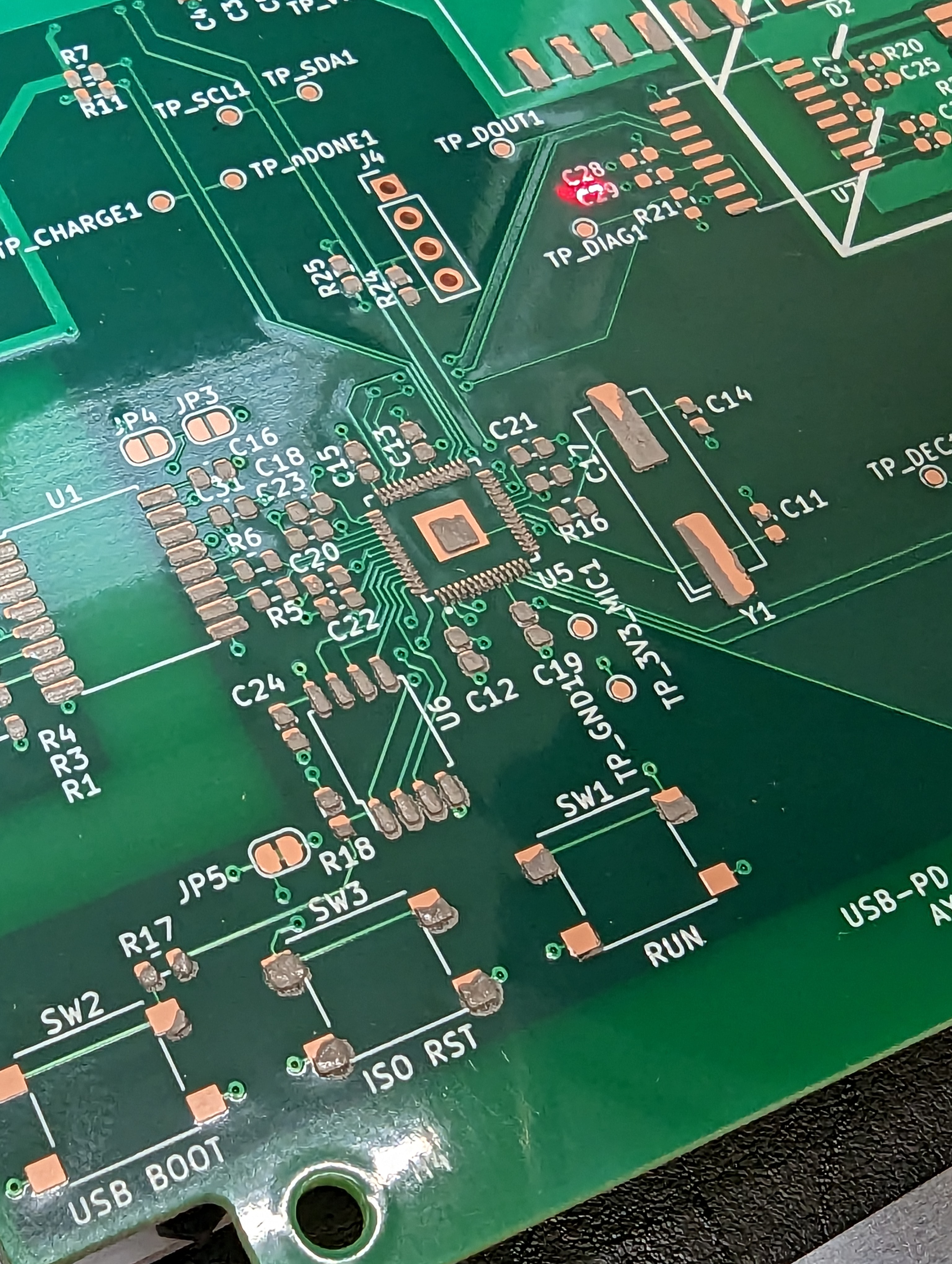
A quick test- most of the paste printed well (look at C12 and C19)

One limitation is that SnBi solder can’t be used with leaded solder, since this can form a Sn-Pb-Bi alloy with a very low melting point (below 100C). And, for some reason, it does not seem to be available in small wire diameters. Hopefully this will change, since having a huge 1mm solder wire sort of prevents any kind of small SMD rework using wire.

Another limitation (as a result of not playing nice with lead) is that leaded pad finishes are inappropriate for SnBi alloys. This, combined with fine-pitch parts, lead me to use OSP. Both leaded and unleaded solder seemed to have less-good wetting on this surface than on ENIG/HASL type finishes. I think that SAC HASL is probably OK for a surface finish but I have not researched it. ENIG would have been preferable for the QFN.

It also seems to take a long time for the solder to get wicked up into solder wick, which can be frustrating. I think a larger tip would help here, but my best “normal size” tip is currently reserved for leaded soldering.

And that’s about it. Overall a good replacement, especially for prototype boards that don’t get hot!

A First Project

I wanted to really see what I could get away with, so I designed a board with a QFN, some fine pitch USB-C connectors, and a handful of of fine pitch leaded SMD components. There were also some larger parts like buttons, crystals, and a whole module, that represent “bulky” parts. To raise the stakes, I decided I would go crazy and use all kinds of $10 ICs.

To solder this, I used the chip-quick NC191LT50, which is a paste that does not need to be refrigerated. It printed nicely using a stainless stencil.

Test run showing bridged pins, some issues wetting

I then put it on the PCB hotplate and took it up to about 160C. Since this is a four layer board, it took a few seconds for the top to heat up. The soldering went surprisingly well, but the QFN had some bridged pins.

Since the solder is low temp, removing the IC was a breeze and the board stayed totally un-scorched. I quickly wiped up some of the solder, and hot-aired it back on. It is now working just fine!

Larger parts were soldered with the same alloy, but with solder wire. I only had a very small soldering iron tip to use (a non-leaded one), so it was hard to get good contact, but the solder did eventually wet everything nicely.

Overall this went shockingly smoothly, given the diversity of parts and using a while new process!

Conclusion: Tin Bismuth Silver solder is here to stay

I am pretty happy with this stuff, especially for projects where a stencil makes sense/is affordable. I’d hate to solder fine pitch components with the huge wire, but I think a paste (even from a syringe) and a hotplate will go a long way.