In my last post I described the challenges in using the LT3750 as a high voltage power supply. Namely, the power supply needs to be restarted after it reaches its target voltage, since it is a one-shot “charger”. An additional problem is that when inspecting the output voltage, it didn’t quite match the calculated output.
Output Discrepancy
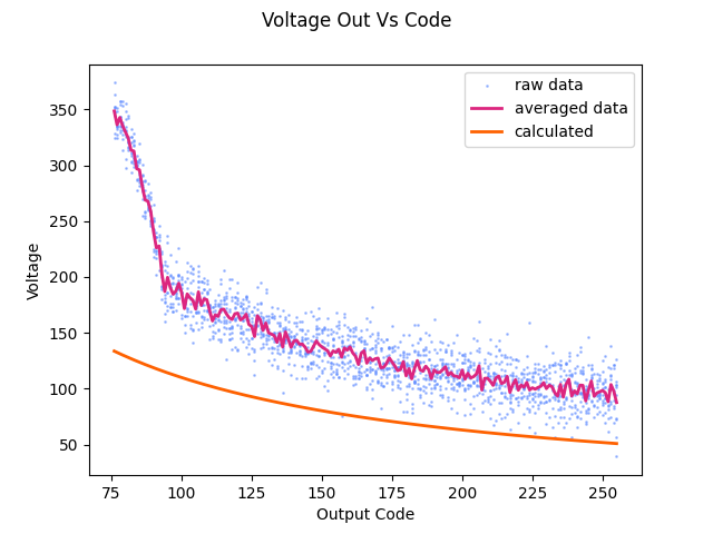
It was surprising to get this plot of expected vs measured output, as reported by the power supply. I would expect some scaling to be wrong, or to have some DC offset due to reworking the voltage divider with 5% resistors instead of 1%, but the hockey stick on the left side of the plot is pretty egregious. Not only do the values take off there, but the concavity of the line actually seems to change! This needed further investigation.
I actually didn’t believe it at first, but after verifying the plot with a few other instruments, and after testing the ADC, rechecking the voltage divider, and a lot of head scratching I realized the problem was in the LT3750, not in the rest of the circuitry.

This was puzzling because on the surface the circuit seemed to do what I expected, aside from the range of 75-100 counts (RBg max = 970 ohms). After scouring the datasheet, I realized that there is a limit on the current into the RVout pin of 1mA. This is not really highlighted in the datasheet. I had calculated a 12k resistor for Rvout in order to get a wide Vout range. However, this violated the rule for for Rvout, and my suspicion is that the proportional current source cant keep up, meaning Vrbg has a hard time overcoming the voltage in the vout comparator, resulting in an overshoot in the output voltage.
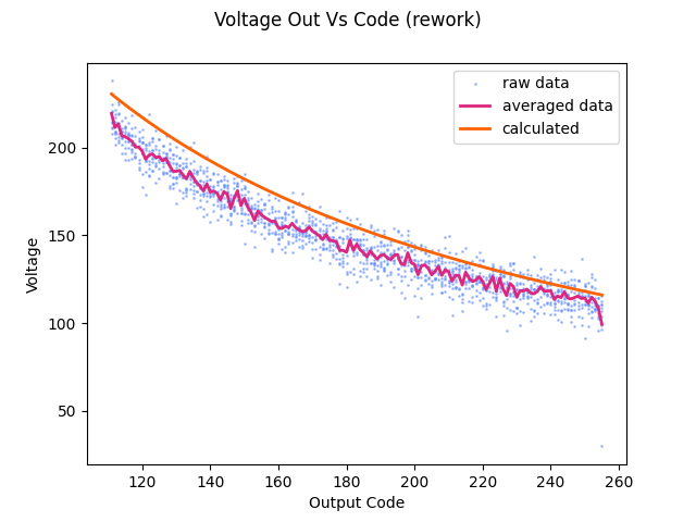
With this hunch, I replaced Rvout with a 27k resistor. This narrowed the usable output range by bringing up the minimum output voltage- ouput voltage is proportional to Rvout/Rbg, so its easy to have a higher voltage. Rbg is limited, per the datasheet, to 2.5k or less. This is annoying, since it would be nice to have a range from about 60V-300V, because my bench supply tops out at 60V. however, at the expected output voltage, the 27k resistor nearly limits the input current to 1mA, so it would be hard to go much smaller.
At least the output is sane now! Ultimately, I could introduce another digipot on the RVout side, but its probably not worth the hassle and the cost of another set of parts for what I want to do with this. The right way to get this power supply might actually be to just use something with continuous feedback to avoid having to kick off another charge cycle.
Output Accuracy:

With the output related to the input, the next step was to relate the potentiometer codes to output voltage. Sadly, this needed to be compared to some instrument, and my multimeter does not have peak hold. So I hooked the supply up to my scope and measured the peak voltage (for a few cycles) per code. I know the expression for the output code is:

Where B is the terminal resistance/parasitic resistance of the digipot (Rbg), and A is a bunch of stuff (turns ratio, a constant, the Rvout resistor value). It doesn’t matter since I am just fitting this curve. The parameters A and B were extracted with scipy, and plugged back into the control code to control output voltage.
Improving ADC reads with rp2040 PIO:

The output stability was initially very bad. This is because the sampling was running very slowly- even running on its own core, reading/writing GPIOs and evaluating expressions takes a lot of time- here you can see the clock rate into the ADC was only 6.7kHz- much lower than the minimum 5 MHz. To put it in perspective, the raspberry pi is only running 6x faster than the max speed that that the adc can be sampled. The slowest sample speed would allow 25 instructions per- reading, including whatever is needed to generate the PWM.
Even at high speeds, it takes a lot of time to get a good sample. Since the output is a bit at a time, each bit only carries one bit of information- this sounds obvious but that means that to get a typical 8 bit resolution, we don’t need to sample 8 bits, we need to sample 256 bits. even running at 20MHz, that still means only one reading every 12.8 microseconds, and that would give worse than 1 volt resolution.
In theory, with proper filtering (which I’m not doing), the adc can provide 16 bit resolution, which is incredible. I decided to settle for taking 12 bits of samples and decimating them, running at about 18 MHz for about a 200 microsecond conversion time (plus some small overhead).
This required using the PIO of the RP2040. PIO is super cool- its like a teeny tiny extra microcontroller that gets run with a tiny(!!!) 9 instruction set. This instruction set is extremely limited- even more so than typical assembly. For example, you can do something like load a number into a 32 bit register, but you cant load a number that is bigger than 31. There is no automatic incrementing of registers, but you can decrement some registers using the jump command. Its a beautiful, but strangely functional (and very fast) mess.
Basically what my code does is load a counter into the y register of how many pwm cycles to do, and loads the maximum number into the x register – 0xFFFFFFFF. Then it starts clocking out pwm cycles, and uses the jump instruction to decrement the x register and y register. When the y register is empty, it reports the x register back to the main program and restarts.

With a little math, this results in how many “high” bits there were in the data. This duty cycle is related back to the read voltage through some simple math from the AMC3306 datasheet and the resistor divider information. This tended to read really high at low voltages (20V when the output was shorted), so I added a correction/adjustment factor to bring it back in line with reality.
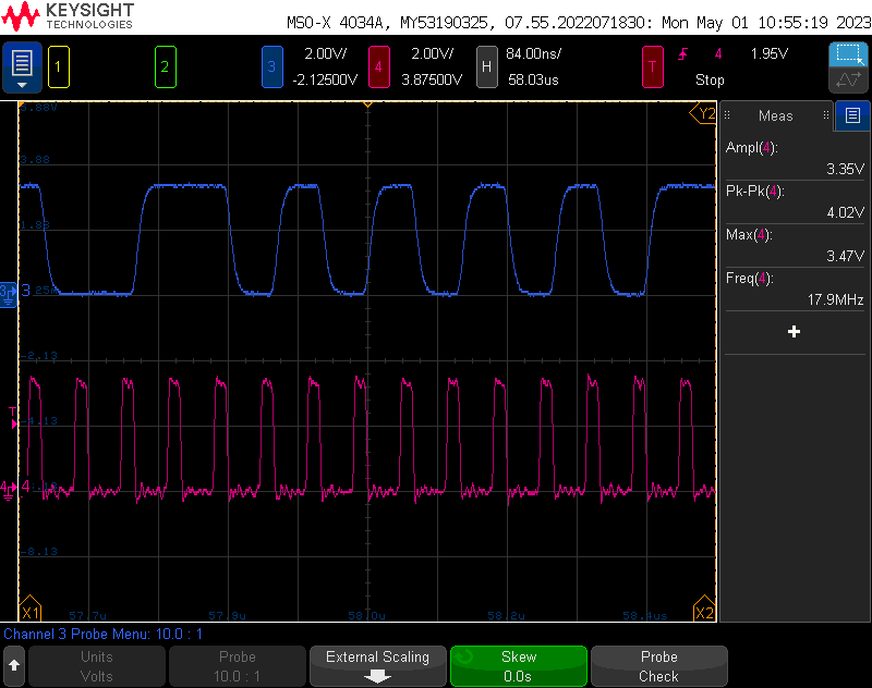
Output Stability:

I wanted to get a very rough idea of the output stability. It’s not easy to to claim any kind of stability or even claim a power output without a variable load of some kind, but I wanted to at least be able to set an output voltage and look at how the supply can regulate against the internal bleeder resistors.
Overall its not too bad- the max is within a volt of the setpoint, and the ripple seems to be about 10V, although given the resolution when zoomed out this far on the scope I am not totally confident in that. Given the hackery and amount of new stuff that went into this, I am satisfied with the outcome.
What I would change:
In the scheme of things, this project went pretty well- I tried at least four or five new processes, so anything working at all is a small miracle. However, there are a couple things I would change if I did it again. Here is a very public bug/ wishlist:
Indicators for hazardous voltage presence, CHARGE and nDone would be neat and blinky. Its nice to have activity indicators. I could actually add most of these with some rework, but it would have been smart to put them on the board!
I do have provisions to add an I2C screen, but no real plans to use it at the moment. This is another nice to have, to get feedback instead of using the console or a dmm, which is limiting. Originally I didn’t expect to use the feedback delta sigma modulator, so this information would not have existed in the system. Now that I have it, it seems silly not to display output voltage.
Increasing the allowable output voltage would also be easy with a substitution of output diode and output caps. It would be wise to choose output caps well in excess of the possible output voltage- even at the expense of space. Currently, my power supply can be commanded (accidentally) to self destruct!
Obviously it would also be great to go back and add the right parts for all the r’s and c’s that are bodged in.
Fix the feedback divider for better range!
PIO errata:
side loading is awesome! it basically allows you a free instruction to set output pins while you do other stuff. The “other stuff” I am doing is nopping, but this could be super useful.
labels at the end of your code will get optimized out. even if they have a nop()[x] after them. however, a regular nop() will keep them in the code.
adc pins used in the pio need to be explicitly enabled in the way you want, e.g. pin = Pin(28, Pin.IN) or pin = Pin(28, Pin.OUT). The PIO state machine class will not do this for you.
