
There are two big electronic questions to answer about the activite:
- Why does the double tap not work well?
- What are all the parts on the board?
I have decided to document my answers to these questions in a narrative form because I think it is interesting to hear how people solve problems.
Double Tap:
It is pretty obvious that the double tapping is going to be sensed by the accelerometer, the ADXL362. Unlike the popular STM accelerometers, the ADXL362 does not have built in double tap detection, although it does have a acceleration-based interrupt that can wake it from sleep. In order to see how the accelerometer was configured, I stuck a logic analyzer on the SPI lines of the device and took several logs of the device in various states, especially power-on and while being tapped.
I used a saleae logic 8 and the logic software to capture the logs and exported them to text files to be parsed by python, which was necessary since each log was several hundred entries long. This made it easy to distinguish between things that are important that change across logs from things that are not important, like slightly different acceleration readings.
The gist of what the device does on startup is:
- turn on the device and read some ID registers
- reset
- Read the registers again, set some thresholds*
- Set up FIFO and FIFO watermark
- Read status until FIFO watermark overflow
- Read FIFO
- Reconfigure FIFO**
The asterisk-ed items are the most interesting, since these are he registers that carry over to the actual operation of the device, and to detecting taps. Since they get reconfigured several times, we need to look at the register states at the very end of all the configuration. It is odd to me to see that the ID registers are poked so much and that the device is reset and read again-it makes it seems like they are using some boilerplate library to set this up.
The relevant registers that have been touched are:
THRESH_ACT_L 0XC7: sets the activity threshold to 199, which is about 1/4 g when FILTERCTL is set to 0x41
FIFO_CONTROL 0X0A: puts the device in stream mode, set MSB in FIFO buffer watermark, and turns off temperature measurement
INTMAP1 0X24: interrupt on pin 1 on either hitting the inactivity threshold or the fifo watermark
INTMAP2 0X10: interrupt pin 2 on hitting the activity threshold
FILTERCTL TO 0X41: +/-4 g range, at 25 hz, half bandwidth off
POWER_CTL 0X02: put into measurement mode
So there you have it- the device is just waiting for a signal of more than a quarter g, and then it will signal the host processor that an activity occurred. But lets dive in a little deeper on the double tapping to see how it is detected.

In practice, we can investigate this behavior with the logic analyzer by sniffing the SPI lines as well as the output pin to the minute hand that moves when you double tap. Circled in blue is the minute hand moving, and in red is the SPI transaction that detected the double tap. The block of transactions in the middle is very similar to the power on interactions mentioned above. I saw this pattern in several instances about 5 seconds before the minute hand ticks.
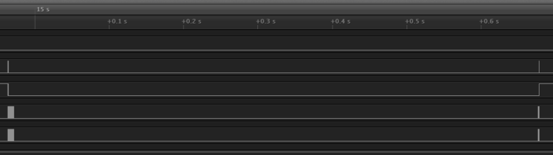
zooming in on the red part shows us that there is a long time where the chip is selected, but not being read. Lets take a look at the accelerometer data from that read.

The pink line is the total acceleration, and the horizontal line is the activity threshold, which the tap threshold is probably greater than. The blue line is the “break” in reads. Since the total number of reads is the whole FIFO, it seems like the window for tapping is at most about 6.8 seconds (512 records % 3 * (1/25Hz)). Likely the window is smaller than that- assuming the break happens right when the second tap is detected, we can see that the window from the last tap to the previous one is about 25 records, or about 1 second.

This is backed up by a second reading, in which the second tap was detected after about 25 readings. This very strict timing and a relatively high acceleration threshold is probably why it is so hard to get the double tapping to work. One thing that could make it easier on users is having a larger or more permissive window, but to only sense tapping one direction- it would reduce the cost of having to sift through 1/3 of the data, and it would probably be less prone to noise. Or you could just do what I did and bang on the face of the watch all day.
What is on the board?

The board is shockingly bare. In the upper left hand corner, there is the NRF51288, and its accompanying crystals (silver). Right below it is an almost invisible ST micro Balun. Just south of the crystals at 9 o’clock is some kind of mystery part with an inductor, or possibly an antenna. South of that looks to be a reverse polarity protection diode. At 6 o’clock is the motor, and at 5 o’clock is the motor driver, marked “1X W48” At 1 o’clock is the ADXL 362 accelerometer, mounted right next to where the chassis PCB is screwed to the case. Just CCW of that looks like some antenna balancing circuitry, but it is hard to be sure.
The really interesting thing is what is not on the board. Very frequently with this kind of product, you will have some kind of voltage converter and a memory chip. And for the relatively higher-current steppers, I would expect to see some kind of h bridge or FETs.
For the pop, it seems like a voltage regulator (or converter) is not needed since there are so few components, and the two heavy hitters on battery usage- the NRF and the ADXL, need to be on in low power sleep or collecting data all the time. Since they sleep so much it is possible that the quiescent current to keep the converter running would overcome the savings in power from running at a lower voltage.
As for memory, this is the AA variant of the chip which has the expansive 256 kB flash (twice the AB variant), but only 16 kB RAM (Half the AC variant). I imagine most of the records are then processed in some way and stored on the chip. This saves on parts, and power on a second chip, but apparently limits the tracking 38 hours between syncs.
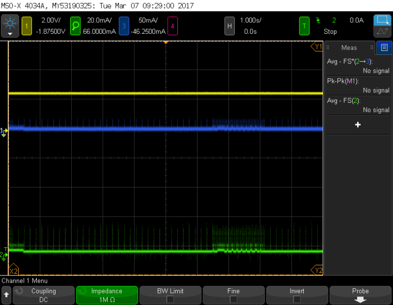
The motors that drive the hands (the movements) are probably driven from the 5mA high-current outputs on the NRF. There can be up to 3 at any given time, meaning that a the NRF can dump a shocking 15mA out at a time, at the battery voltage. This is consistent with reports form users that at the end of the battery life, the hands stop working, even though the watch knows what time it is. At the end of the battery’s life, the voltage will drop, and less power will be delivered to the motor- some of these motor movements will fail, and the clock face will be wrong. Above you can see the current output (green line) from driving the motor- the peaks are around 15 mA above the “floor”.

On the other hand, the motor is too large for the NRF to handle, so some kind of FET arrangement is used to drive it. It takes 60 mA (peak) from the battery! That is why setting a lot of alarms is taxing on the device.
Final Thoughts:
This is a pretty simple electronics-wise for such a sophisticated device, which speaks volumes about the team that designed and built it- it is pared down to the absolute minimum complexity, with only the barest of sensor packages. Yet I feel the device does deliver on what it promises to do.

Hello. It’s AMAZING analysis! They finally fixed the problem with doubletap by making it tripletap))) in 1600 firmware, but remove this option totally in the last one 1910. It works smoothless, until i occasionally upgrade my watches. Now i’m trying to downgrade over JTAG/SWD. Maybe you know which of testpoints is SWDIO and SWDCLK? Thank you.