
With the ADSXXXX series out of stock for the foreseeable future, I needed to evaluate the ADC’s on several micros to understand if they would be good enough for my application – reading oxygen sensors. Mostly I care about DC characteristics, because my signal should be changing very slowly- on the order of many seconds.
I’ve seen a lot of interesting work done on ADC characterization and calibration, but only rarely do the posts explain where the reference voltage is coming from. If the voltage source is noisy or has some nonlinearity or bias, it will throw off the calibration.
really really excellent series on adc error/calibration from thea.codes
demo showing how the esp32 adc is bad
The most obvious way to do this is to generate a really nice (precise + accurate) voltage, put it into the ADC, and then figure out what the expected error is for a sample or for multiple samples. With enough resolution on this voltage, I can look for missing codes (high DNL) and for error in value from code-to-code (INL), and find really good gain and offset correction factors, and come up with an idea of how good the ADC is (at DC, for some ADC settings, etc).
The trick, of course is generating the nice voltage. Since I don’t have a sub-mv programmable reference voltage, I had to buy one. Since I didn’t want to spend hundreds of dollars on a non-programmable benchtop equipment, I decided to buy a 16-Bit DAC. These chips are pricey, but on the order of a pastry and a coffee, not a nice bicycle or oscilloscope. Instead of spinning my own board, I bought an eval kit to speed things up.
The DAC8050X comes in a one and two channel flavor. I got the two channel flavor in case I wanted to make differential measurements at some point in the future. These are really nice, and offer <1LSB nonlinearity. This is really pretty impressive to me, and looking at the typical characteristics, the INL and DNL are way way lower than 1 LSB.
The DAC80502 is also pretty sweet in that it has programmable gains for both the reference and the outputs- this gives it a really wide range of outputs, without any external circuitry. It also has an external VREF in, so you can supply a voltage range you care about. Combining the two outputs with some creative-op amp-ery could give you a really wide range of voltages to play with, but I really care most ab out the sub-3v range, which this is perfect for.
*this seems somewhat sketchy given the really bad stated INL/DNL for the adc, and the fact that the DAC on the esp32 seems to be 8bit. it might make the output look linear, but I wouldnt use it for anything important
Who tests the Tester?:
When making measurements against a standard, its important to understand how good your reference is. In this case the DAC is being used as a reference, which means it needs to be very “nice”. There are many charts in the datasheet, showing that all kinds of systematic and thermal drift, referred noise, error under load, etc. The total unadjusted error appears to be around .02% typically, and the INL/DNL per code is <<1 bit, usually around .2 LSB. While these charts are all very reassuring, its nice to verify them.
To do this I connected the DAC to a nice 6.5 digit multimeter (Agilent 34465a) and captured a 5 reads at each output code, and then calculated the error per code, to verify. This turned out to be a slow process, because 2^16 (65.5k) times even a few milliseconds is a LONG time. In order for the instrument to have a high enough resolution/accuracy, I had to wait a long time for it to collect data, so the test ended up taking ~4 hours.
N.B. the 34465A is a lot faster at resolving lower voltages than the lower spec models- those would have taken even longer!

This chart shows the measured voltage and the difference in voltage from output code-to-code in LSB. The ideal difference code-to-code should be 1LSB of voltage – 1 LSB is Vref/(2^16). A difference of 0 indicates no change in output (a missing output code) and the distance from 1LSB indicates how far from the ideal each step is (INL). A different-sign difference between codes, which we don’t see here, indicates that the output is not monotonic (increasing or decreasing constantly). Fortunately, the worst thing seen are some missing codes at the start.
NB: this happens even without auto-zero on, and the meter can read negative voltages, so these really are missing codes (DNL>1). This seems wrong compared to the datasheet, but my measurements should be good enough to capture this. That said, I wont totally rule out some small dc offset or error in measurement.

That means this DAC is pretty awesome. The standard deviation of the errors is about .073 LSbs. Its not quite gaussian (kurtosis 1.17) because it has basically no tails, but its close enough for me. As you can see the LSB error code to code (DNL) is usually less than .2, which matches with the datasheet.
NB: this result was obtained under ideal circumstances. When I worked at my computer/charged my phone right next to it and generally jostled the setup, I got non-monotonic readings an more LSB error. With short wires to the DMM and good test practices it performed much better.
Preliminary Data:
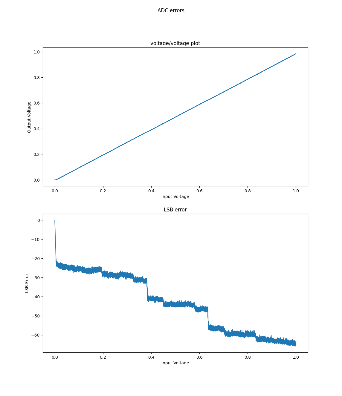
Here is a read of the SAMD21 ADC with the internal 1VREF and no gain, compared to the DAC with 1.25VREF. The total error/code is shown below in LSB. This is a lot more than the stated 15 bit total unadjusted error, but I haven’t used the built in gain/offset correction, and I’m not sure if this incorporates the samd21 adc arduino bug. As you can see, a simple offset could reduce this total error by about 40%. Interestingly, there were a couple very odd codes near the 1/3 and 2/3 points where the error quickly jumps.
