After my first dactyl, I decided I needed at least another one, maybe two for my home, my office, and some third place. Unfortunately, instead of just sucking it up and wiring it by hand, I had the delusional notion that it would take less time for me to make a flex PCB to do the wiring for me.
Design Process
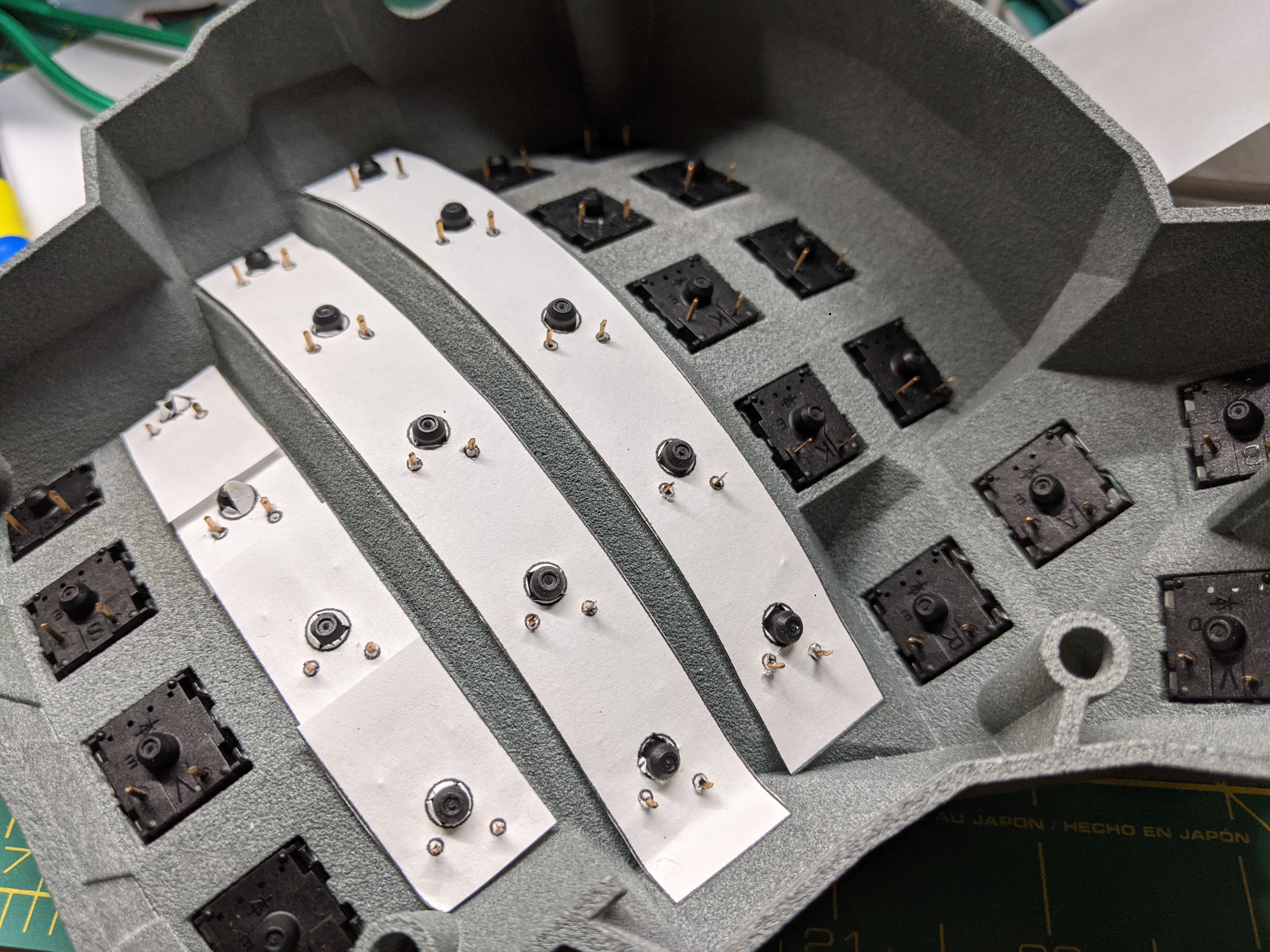
My initial design process was to do a quick paper prototype. To do this I printed out (on a 2d printer) a lot of 1u sized pieces of paper and fit them to an empty dactyl shell. bridges were added to these connections, and the whole thing was scanned on a flatbed scanner. after a few iterations I had a pretty organic board that fit pretty nicely, but ultimately it was going to drive the price up because it did not use board area efficiently, and it was going to bump me out of a lower price bracket.

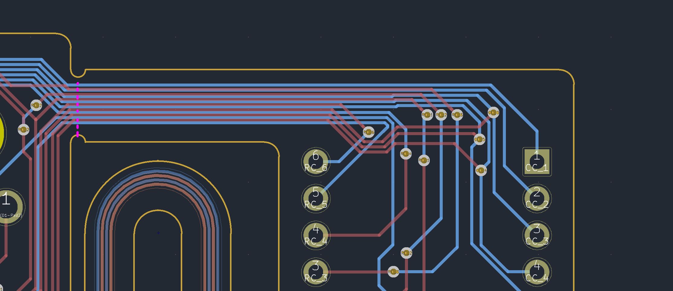
The original design helped me work out some of the main layout challenges around the thumb cluster, which was helpful for the next iteration. Unfortunately, the organic shape made the flex quite inefficient in space usage. Instead of trying to get a flex that would conform exactly to the shell, I realized the main spacing issue was between columns (keys are spaced about 23 mm vertically). To simplify routing, I decided there would be a single connector between columns, with a few specialized connectors for the thumb cluster and the ‘extra keys’.
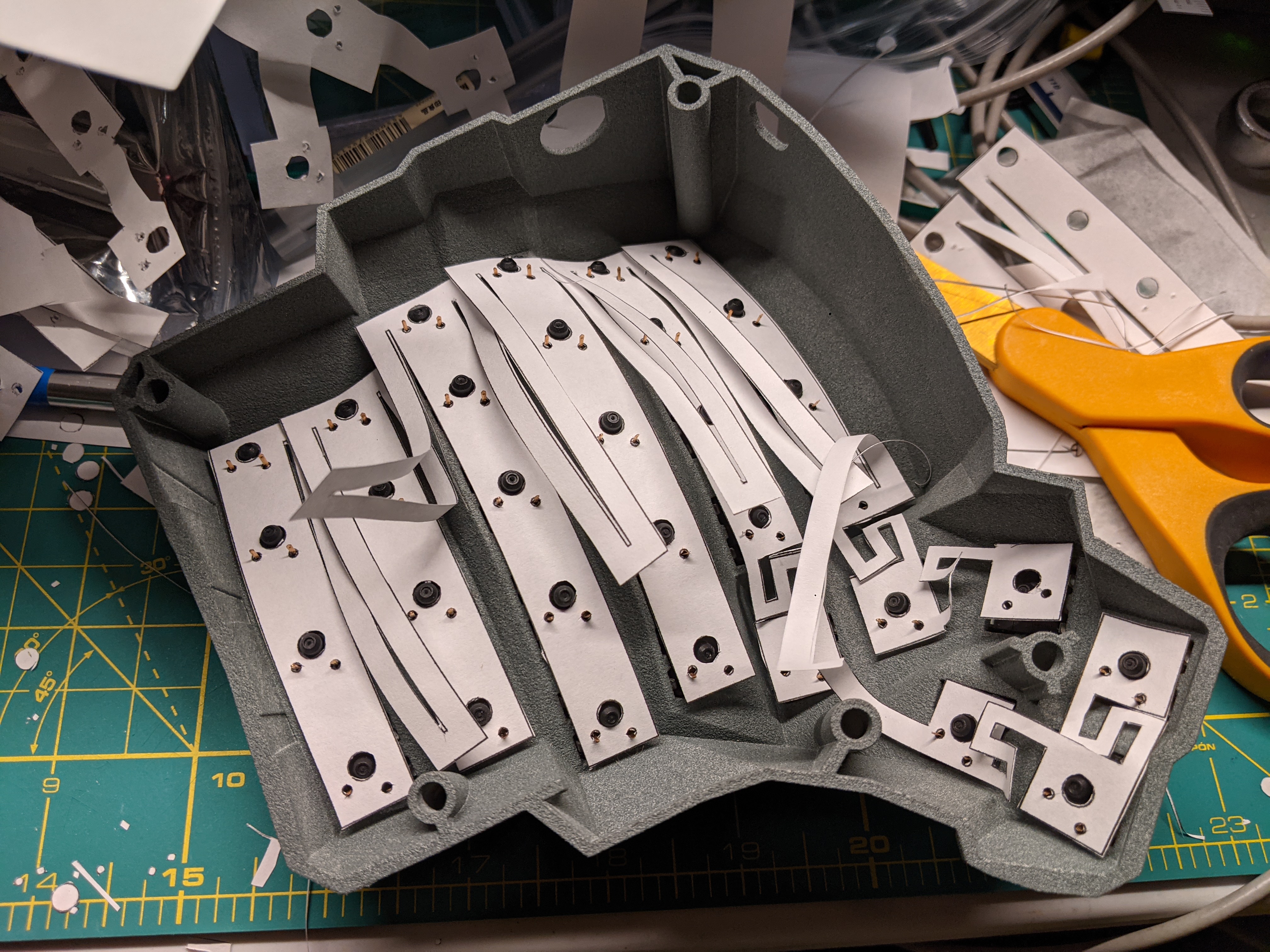


I went back and forth between physical prototypes, electrical layouts, and sketches to arrive at this final shape. Paper cutouts are a cheap and fast way to design, and making a physical model gives me a lot more confidence in terms of clearances (especially for assembly). Doing this in a CAD model would have been possible, but nightmareish, due to the curvature and odd angles of the switch connectors.

Here is the final version! Since its a pain to make the actual flex parts of the pcb in kicad, I tried to minimize unique flex connection types.
Kicad Minutiae
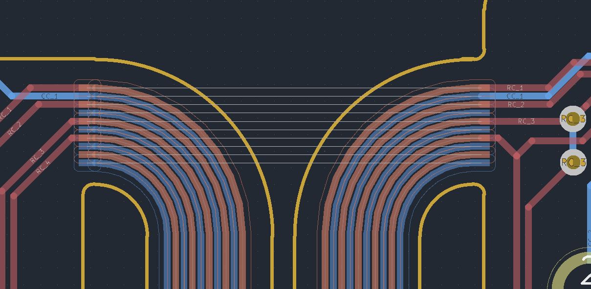
The inter-column connector design was refined over time, and it let me make sure I had the right number of interconnects between columns. Due to constraints in kicad in routing arcs, the actual flex had to be laid out and then converted to a pad footprint in the footprint editor. this means the flex tracks are represented as parts on the schematic, which is a little annoying because it makes the nets not work for DRC errors/net connections, as each pad can only have one anchor. It also made it a little irritating to change routing, because the actual footprint/schematic needed to be changed to make a routing change. On the other hand, I was guaranteed identical routing between all my interconnects.
Flex Details
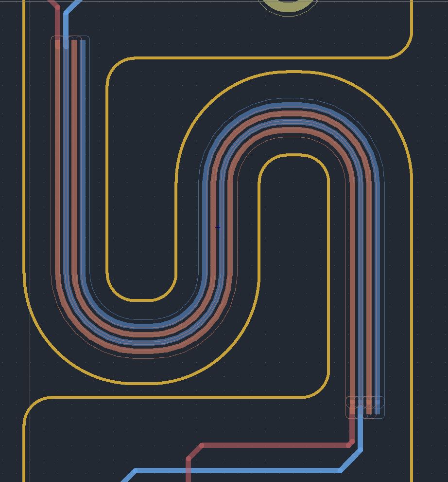
There are a few little flex details that I threw in, which I hope help make the board more functional mechanically. As you can see above, the main flex parts were routed without overlapping copper to prevent the thicker copper (copper-kapton-copper standwich) from stiffening the flex. I also tried to add maximum radii on the parts that would flex.
Here you can see the bridge where traces go to the microcontroller. on this flex, there are a couple notches which should help define a board flex location.
Diodes were placed to minimize the stress on the solder joints by putting them perpendicular to the flex direction.
Production
Well…its ordered. The rest of the keyboard parts are in hand, so I am hoping to have another keyboard in a few weeks, with a lot less wiring!
