
Misfit Flash Teardown!
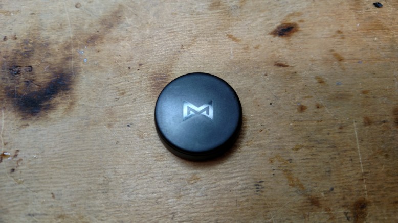
I was at an REI garage sale and found a Misfit Flash for 10 bucks. I always loved the Misfit deadfront displays, so I picked it up figuring it would be fun to take apart, especially since I work at a company that specializes in connected devices. I was surprised when I got home and realized that there is a big difference between the ultra-cool shine, and the much more economical flash. I still learned a lot and I am glad I got to dive into some hardware that did not already have several big teardowns.
Mechanical

Battery, PCB and ring, and bottom
The engineering in the flash is as minimalist as its design. The almost featureless puck sits about 6mm high and is about 25mm across. Most of the space is taken up by a battery, which is installed by popping the bottom cover off.
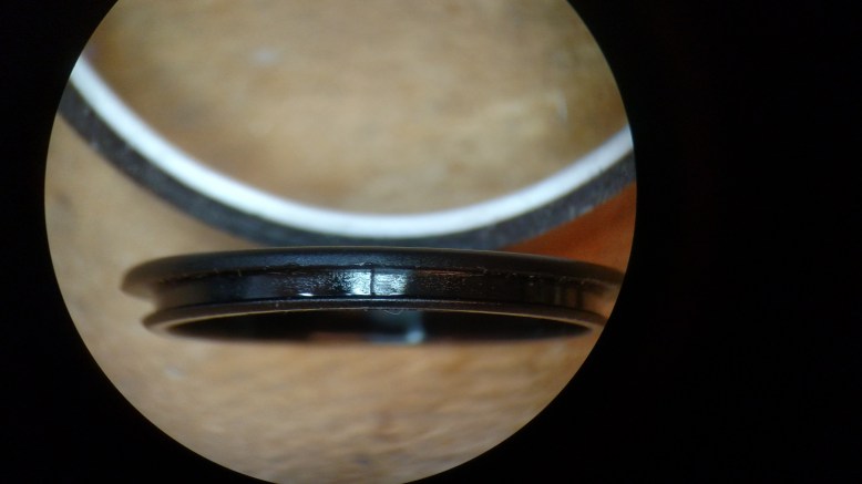
The bottom cover is held in by an annular snap, which is sealed against water by an o-ring that runs around its perimeter. The snap is molded with two external actions, as you can see from the flash in the groove. The material is almost without a doubt ABS.


Under the battery cover is the battery, which is attached to the PCB. To prevent the PCB from falling out, a ring of plastic is heat staked to the “top” plastic which retains the PCB. This is super obvious in the rightmost photo, where you can see that the case was accidentally melted by the heat stake tool.

I used a razor knife (x-acto #11) to sneak under the ring and cut out the heat stakes. This let me pop the PCB out after I removed the ring. The ring is a really small part, but it is important for holding in the PCB, locating the battery and protecting the battery clips!


This leaves the flash at a grand total of three molded parts- but one is a little more complicated than the others. This is the “face” of the device, which is a translucent, soft-touch plastic (santoprene maybe?) overmolded on a thin piece of ABS. This outer layer allows the fairly bright LEDS to shine through tiny holes in the ABS, creating a crisp dot on the face of the device. In the left photo you can see thin walls of the darker soft-touch material in the light wells. This is was caused by clearance between the ABS insert and the tool that held it.

The overmolding was done carefully to minimize the impact it had on the cosmetic outer surface. It looks like this edge was used for injecting the plastic, and it was carefully trimmed away later. The rest of the edge is totally smooth.
Electrical
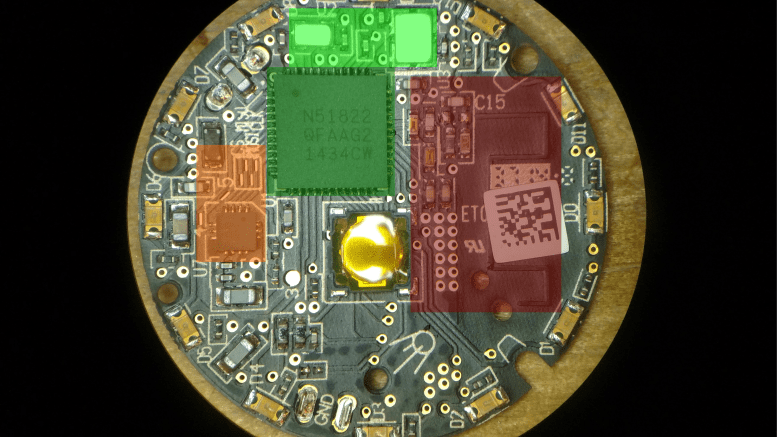
Orange: accelerometer, light green: Crystals, dark green: NRF51822 AA model, dark red: RF antenna and balancing network
Compared to something like a phone, there is not a lot going on, but that is not to say that it is not complicated. On the east side of the board, you can see the RF block and antenna. To the north, you see a couple of crystals. The west side is dominated by a QFN which is likely an accelerometer. Right in the middle, there is a button, and on the south end of the board there is a happy little sputnik.

On the back side of the board, there is a battery holder, a tag-connect 10 pin header, and a nice silkscreen that says it was designed in San Fransisco, along with the initials AR and GR- maybe the initials of the people who did the layout. When in use, most of this is covered by a big sticker, but I love seeing cool little details like this.
In any battery operated product, less is more. The flash uses a CR2032 coin cell, which boasts a lofty 225 mAh at 3 volts. The best AA you can buy in stores- the energizer L91- has about six times as much energy, although comparing batteries is like trying to compare apples to bread- they both have calories but they are processed in very different ways.
To achieve its quoted 6 month lifespan, this means that it has a whopping 15 joules per diem to spend. That’s insanely low- to put it in perspective, that’s the same amount of energy as it takes to lift a bag of about 7 apples from the floor to the top of the fridge. Another way to put it would be 1/30,000 th of the kcalories in an apple. Anyway, the device has to be designed very carefully to use such a small amount of power.
The most radical part of the power saving strategy is to actually have no voltage regulator. Many devices have started to use very efficient switching power converters to regulate power, allowing all devices to operate at the voltage they are most efficient at. However, these converters come with three major costs- money, board space, and quiescent current (power consumed when the converter is idle). The designers of this board decided to eschew converters, and just choose parts with a wide voltage range, from 1.8V-3V+.

The accelerometer is most likely the LIS2DH from ST Micro. Adafruit and Sparkfun both mentioned it on their teardowns of the shine, and the package is the same. The pinout is also identical to what I saw labeled on the board (see photo) in terms of an SPI connection between the microcontroller and the chip. NB that SPI has a power savings over I2C in terms of not needing pull up resistors.

The choice to use red leds on the flash is not because it looks cool or sinister, but because much like the the other major components, red LEDs will still work at low voltages. While or blue LEDs require almost 4V to work, while a nice green led would be in the range of 2.2V. Red leds have the lowest voltage drop of any color of led, at around 1.7 volts, although they are quite a bit dimmer at low voltages. This means they will operate down to about the voltage level that the accelerometer does.


At the heart of the device is the beloved NRF51822. This is a frontrunner in terms of low power bluetooth, with plenty of development kits and even cheap pre-certified modules. This SoC combines a 32 bit Arm Cortex-M0 with a power sipping 2.4Ghz transceiver. This is the brain of the device. Around it, there are a couple of crystals, one at 16 Mhz and one at 32 Mhz. These allow the chip to sleep at low power for long periods of time. Also in the constellation of parts surrounding the NRF is an antenna balancing network, and a trace antenna.
Final Thoughts
The Misfit Flash is a neat thing. I mean that in the fullest sense of the word- it is tidy. Everything is neatly connected, and everything has a purpose, and the effect is a simple and attractive object. I never used it for fitness tracking, but I did have a lot of fun just playing with it and watching the LEDS blink. People who are designing connected hardware would do well to study this exercise in minimalism.

What a fantastic article! This is tear down is really full of incredible valuable information. Keep on your good work.